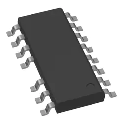
Images are for reference only
10M16SCU324C8G
IC FPGA 246 I/O 324UBGA
- Manufacturer
- Mfr. Part #10M16SCU324C8G
- Package 324-LFBGA
- Datasheet
- In Stock6731
100% Original & New
24 Hours ready to ship
365 Days Warranty
RFQ & Get more Discounts
Specifications
| Package | Tray |
| Series | MAX® 10 |
| ProductStatus | Active |
| NumberofLABs/CLBs | 1000 |
| NumberofLogicElements/Cells | 16000 |
| TotalRAMBits | 562176 |
| NumberofI/O | 246 |
| Voltage-Supply | 2.85V ~ 3.465V |
| MountingType | Surface Mount |
| OperatingTemperature | 0°C ~ 85°C (TJ) |
| Package/Case | 324-LFBGA |
Overview
Description
This FPGA integrates flash memory, allowing for efficient reconfiguration without external memory components, which simplifies design and reduces costs. The "324" refers to the package type—specifically, a 324-pin BGA (Ball Grid Array) package, facilitating a compact design and ease of integration into printed circuit boards.
The 10M16SCU324C8G supports various I/O standards, making it adaptable for different interface protocols, and it is accompanied by robust development tools for streamlined design processes. Its low power consumption and high-performance capabilities make it ideal for applications requiring both efficiency and processing power.
Features
1. Logic Elements: It contains up to 16,000 logic elements, allowing for complex digital designs.
2. Memory: Integrated RAM blocks offer up to 576 Kbits of memory for data storage.
3. I/O Pins: Features 324 user I/O pins with support for multiple I/O standards, enabling versatile interfacing options.
4. Embedded Flash: It has an on-chip flash memory, allowing for configuration storage and fast reconfiguration.
5. Analog Features: Includes built-in analog-to-digital converters (ADCs) for mixed-signal applications.
6. Low Power Consumption: Designed for low power operation, making it suitable for battery-powered applications.
7. Single Voltage Operation: Operates at a single voltage level (3.3V), simplifying design and power supply requirements.
These features make the 10M16SCU324C8G suitable for a wide range of applications, including automotive, industrial, and consumer electronics.
Package
Pinout
The pins on the 10M16SCU324C8G serve multiple functions, including:
1. I/O Pins: Configurable input/output pins for interfacing with external devices.
2. Power Pins: Supply voltage and ground connections.
3. Clock Pins: Dedicated clock inputs and outputs for timing control.
4. Configuration Pins: Used for programming and configuration of the FPGA.
5. JTAG Pins: For boundary scan and debugging purposes.
These pins can be assigned to specific functions based on the design requirements, making the FPGA versatile for numerous applications in embedded and digital design.
Manufacturer
Application
Equivalent
Shipping
Shipping MethodsWe
offer global shipping services through DHL, FedEx, TNT, UPS, or any other forwarder of your choice.
Shipping Fee Reference (DHL/FedEx):
DHL: Shipping cost ranges from $25-$45 (0.5kg), with an estimated delivery time of 2-5 business days.
FedEx: Shipping cost ranges from $25-$40 (0.5kg), with an estimated delivery time of 3-7 business days.
UPS: Shipping cost ranges from $25-$45 (0.5kg), with an estimated delivery time of 3-7 business days.
TNT: Shipping cost ranges from $25-$65 (0.5kg), with an estimated delivery time of 3-7 business days.
EMS: Shipping cost ranges from $30-$50 (0.5kg), with an estimated delivery time of 7-15 business days.
Registered Air Mail: Shipping cost is $2-$4 (0.1kg), with an estimated delivery time of 5-20 business days.
Payments
Payment Methods
The Payment term is 100% Prepaid.
Currently, we only accept the below payment methods:
1. PayPal
2. Credit/ Debit Card
3. Wire Transfer
Similar
-
![MX25R8035FM1IL0]() MX25R8035FM1IL0
MX25R8035FM1IL0
Macronix
-
![MX25V1635FZNQ03]() MX25V1635FZNQ03
MX25V1635FZNQ03
Macronix
-
![MX30LF2G28AD-TI]() MX30LF2G28AD-TI
MX30LF2G28AD-TI
Macronix
-
![MX25R6435FBDIL0]() MX25R6435FBDIL0
MX25R6435FBDIL0
Macronix
-
![MX25L25673GMI-10G]() MX25L25673GMI-10G
MX25L25673GMI-10G
Macronix
-
![MX25U51279GXDR00]() MX25U51279GXDR00
MX25U51279GXDR00
Macronix
-
![MX25U25643GZNI00]() MX25U25643GZNI00
MX25U25643GZNI00
Macronix
-
![MX25L6433FM2I-08G]() MX25L6433FM2I-08G
MX25L6433FM2I-08G
Macronix
-
![MX25L12833FM2I-10G]() MX25L12833FM2I-10..
MX25L12833FM2I-10..
Macronix
-
![MX25L25645GXDI-08G]() MX25L25645GXDI-08..
MX25L25645GXDI-08..
Macronix
-
![MX25L25735FMI-10G]() MX25L25735FMI-10G
MX25L25735FMI-10G
Macronix
-
![MX30LF4G18AC-TI]() MX30LF4G18AC-TI
MX30LF4G18AC-TI
Macronix