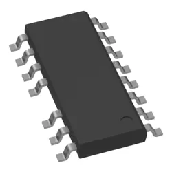
Images are for reference only
5M40ZE64C5N
IC CPLD 32MC 7.5NS 64EQFP
- Manufacturer
- Mfr. Part #5M40ZE64C5N
- Package QFP-64
- Datasheet
- In Stock3971
100% Original & New
24 Hours ready to ship
365 Days Warranty
RFQ & Get more Discounts
Specifications
| Package | Tray |
| Series | MAX® V |
| ProductStatus | Active |
| ProgrammableType | In System Programmable |
| DelayTimetpd(1)Max | 7.5 ns |
| VoltageSupply-Internal | 1.71V ~ 1.89V |
| NumberofLogicElements/Blocks | 40 |
| NumberofMacrocells | 32 |
| NumberofI/O | 54 |
| OperatingTemperature | 0°C ~ 85°C (TJ) |
| MountingType | Surface Mount |
| Package/Case | 64-TQFP Exposed Pad |
Overview
Description
Key specifications include a 5,000 logic element count, embedded memory blocks, and digital signal processing (DSP) capabilities, enabling efficient processing of complex algorithms. The device supports various I/O standards and provides flexible interfacing options.
Additionally, the 5M40ZE64C5N integrates a built-in phase-locked loop (PLL) for clock management and offers the ability to program the FPGA using standard hardware description languages like VHDL and Verilog. Its versatility allows it to be used in applications like motor control, data acquisition, and video processing. Overall, it is a powerful tool for developers seeking to implement custom logic in a compact and efficient package.
Features
1. Logic Elements: It integrates up to 40,000 logic elements, providing ample resources for diverse designs.
2. Embedded Memory: Offers up to 2.5 MB of embedded RAM, facilitating efficient data storage and processing.
3. I/O Support: Supports up to 64 I/O pins with various voltage standards, ensuring compatibility with multiple interfaces.
4. DSP Blocks: Equipped with DSP (Digital Signal Processing) blocks for high-performance arithmetic operations.
5. Non-Volatile Memory: Incorporates Flash memory for configuration storage, allowing for instant-on capabilities and reducing boot time.
6. Power Efficiency: Features low static and dynamic power consumption, making it suitable for battery-operated applications.
7. Development Tools: Compatible with Intel's Quartus Prime software for easy design and simulation.
The 5M40ZE64C5N is ideal for applications in industrial control, automotive, and consumer electronics, offering a balance of performance and flexibility.
Package
Pinout
- Configurable I/O Pins: Supports various I/O standards for interfacing with other devices.
- Logic Elements: Contains adaptive logic modules for implementing custom logic designs.
- Embedded Memory: Offers on-chip memory blocks for data storage and processing.
- DSP Blocks: Includes dedicated resources for digital signal processing tasks.
- JTAG Interface: Allows for programming and debugging.
The 5M40ZE64C5N is suitable for applications in telecommunications, automotive, and consumer electronics, providing flexibility in design and low power consumption.
Manufacturer
Application
Equivalent
Shipping
Shipping MethodsWe
offer global shipping services through DHL, FedEx, TNT, UPS, or any other forwarder of your choice.
Shipping Fee Reference (DHL/FedEx):
DHL: Shipping cost ranges from $25-$45 (0.5kg), with an estimated delivery time of 2-5 business days.
FedEx: Shipping cost ranges from $25-$40 (0.5kg), with an estimated delivery time of 3-7 business days.
UPS: Shipping cost ranges from $25-$45 (0.5kg), with an estimated delivery time of 3-7 business days.
TNT: Shipping cost ranges from $25-$65 (0.5kg), with an estimated delivery time of 3-7 business days.
EMS: Shipping cost ranges from $30-$50 (0.5kg), with an estimated delivery time of 7-15 business days.
Registered Air Mail: Shipping cost is $2-$4 (0.1kg), with an estimated delivery time of 5-20 business days.
Payments
Payment Methods
The Payment term is 100% Prepaid.
Currently, we only accept the below payment methods:
1. PayPal
2. Credit/ Debit Card
3. Wire Transfer
Similar
-
![MX25V5126FM1I]() MX25V5126FM1I
MX25V5126FM1I
Macronix
-
![MX25V2033FM1I]() MX25V2033FM1I
MX25V2033FM1I
Macronix
-
![MX25R3235FZNIL0]() MX25R3235FZNIL0
MX25R3235FZNIL0
Macronix
-
![MX25V16066M2I02]() MX25V16066M2I02
MX25V16066M2I02
Macronix
-
![MX30LF2G28AD-TI]() MX30LF2G28AD-TI
MX30LF2G28AD-TI
Macronix
-
![MX25R6435FBDIL0]() MX25R6435FBDIL0
MX25R6435FBDIL0
Macronix
-
![MX29GL512FHXFI-11G]() MX29GL512FHXFI-11..
MX29GL512FHXFI-11..
Macronix
-
![MX25U25645GXDI00]() MX25U25645GXDI00
MX25U25645GXDI00
Macronix
-
![MX29LV160DTTI-70G]() MX29LV160DTTI-70G
MX29LV160DTTI-70G
Macronix
-
![MX25L25645GXDI-08G]() MX25L25645GXDI-08..
MX25L25645GXDI-08..
Macronix
-
![MX25L25735FMI-10G]() MX25L25735FMI-10G
MX25L25735FMI-10G
Macronix
-
![MX30LF4G18AC-TI]() MX30LF4G18AC-TI
MX30LF4G18AC-TI
Macronix