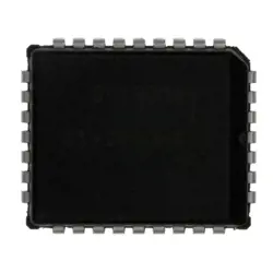
Images are for reference only
74AHCT125PW
Logic Gates
- Manufacturer
- Mfr. Part #74AHCT125PW
- Package
- Datasheet
- In Stock8501
100% Original & New
24 Hours ready to ship
365 Days Warranty
RFQ & Get more Discounts
Specifications
Overview
Description
Each buffer accepts standard TTL input levels and provides CMOS output levels, making it compatible with various logic families. The device has a high-speed operation with propagation delays typically around 6.5 ns at 5V. The 74AHCT125PW also includes a tri-state output feature that allows for the control of data flow on shared lines, enhancing the versatility of circuit designs.
The IC is packaged in a 14-pin TSSOP format, making it suitable for space-constrained applications. It's often used in data routing, signal buffering, and interfacing between different logic levels in digital systems.
Features
1. Quad Configuration: Contains four independent buffer/driver circuits.
2. Three-State Outputs: Outputs can be driven high, low, or placed in a high-impedance state, allowing for bus applications.
3. High-Speed Operation: Operates at a maximum frequency of up to 125 MHz, suitable for high-speed digital applications.
4. Voltage Compatibility: Designed to operate with a wide supply voltage range from 4.5V to 5.5V, making it compatible with various logic levels.
5. Low Power Consumption: Consumes low static and dynamic power, enhancing energy efficiency.
6. TTL Compatibility: Compatible with TTL (Transistor-Transistor Logic) levels, ensuring integration with other TTL devices.
7. Wide Temperature Range: Functioning temperature range from -40°C to 125°C, suitable for industrial applications.
8. Available in Surface-Mount Package: Offered in a TSSOP package (PW), facilitating compact designs.
This device is ideal for buffering data signals in a variety of digital circuits, including communication systems and microcontroller interfacing.
Package
Pinout
- Pins 1-4: Outputs (Y1, Y2, Y3, Y4)
- Pins 5-8: Inputs (A1, A2, A3, A4)
- Pins 9-12: Enable inputs (OE1, OE2, OE3, OE4)
- Pin 13: Ground (GND)
- Pin 14: VCC (Power supply)
- Pins 15-20: Additional outputs and inputs
The function of the device is to buffer and drive signals, providing high-speed operation with TTL compatibility. The outputs are enabled or disabled based on the state of the enable pins (OE), allowing for control over signal flow in digital circuits.
Manufacturer
Application
Equivalent
1. 74HC125
2. 74HCT125
3. 74LVC125
4. 74ACT125
Ensure to check the specific voltage levels and speed requirements for compatibility in your application.
Shipping
Shipping MethodsWe
offer global shipping services through DHL, FedEx, TNT, UPS, or any other forwarder of your choice.
Shipping Fee Reference (DHL/FedEx):
DHL: Shipping cost ranges from $25-$45 (0.5kg), with an estimated delivery time of 2-5 business days.
FedEx: Shipping cost ranges from $25-$40 (0.5kg), with an estimated delivery time of 3-7 business days.
UPS: Shipping cost ranges from $25-$45 (0.5kg), with an estimated delivery time of 3-7 business days.
TNT: Shipping cost ranges from $25-$65 (0.5kg), with an estimated delivery time of 3-7 business days.
EMS: Shipping cost ranges from $30-$50 (0.5kg), with an estimated delivery time of 7-15 business days.
Registered Air Mail: Shipping cost is $2-$4 (0.1kg), with an estimated delivery time of 5-20 business days.
Payments
Payment Methods
The Payment term is 100% Prepaid.
Currently, we only accept the below payment methods:
1. PayPal
2. Credit/ Debit Card
3. Wire Transfer
Similar
-
![MX25L3233FZBI-08Q]() MX25L3233FZBI-08Q
MX25L3233FZBI-08Q
Macronix
-
![MX25V16066M2I02]() MX25V16066M2I02
MX25V16066M2I02
Macronix
-
![MX30LF2G28AD-TI]() MX30LF2G28AD-TI
MX30LF2G28AD-TI
Macronix
-
![MX25L8035EM2I-10G]() MX25L8035EM2I-10G
MX25L8035EM2I-10G
Macronix
-
![MX25R6435FBDIL0]() MX25R6435FBDIL0
MX25R6435FBDIL0
Macronix
-
![MX25U51279GXDR00]() MX25U51279GXDR00
MX25U51279GXDR00
Macronix
-
![MX25L2006EM1I-12G]() MX25L2006EM1I-12G
MX25L2006EM1I-12G
Macronix
-
![MX25U6435FM2I-10G]() MX25U6435FM2I-10G
MX25U6435FM2I-10G
Macronix
-
![MX25L12833FM2I-10G]() MX25L12833FM2I-10..
MX25L12833FM2I-10..
Macronix
-
![MX29F040CQI-70G]() MX29F040CQI-70G
MX29F040CQI-70G
Macronix
-
![MX29F040CTI-70G]() MX29F040CTI-70G
MX29F040CTI-70G
Macronix
-
![MX29F800CBTI-70G]() MX29F800CBTI-70G
MX29F800CBTI-70G
Macronix