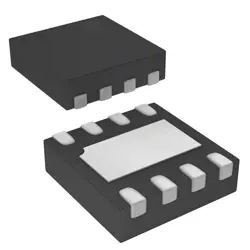
Images are for reference only
74AUP1G74DC
- Manufacturer
- Mfr. Part #74AUP1G74DC
- Package
- Datasheet
- In Stock2870
100% Original & New
24 Hours ready to ship
365 Days Warranty
RFQ & Get more Discounts
Specifications
| Brand | Nexperia |
| Product Type | Flip Flops |
| Subcategory | Logic ICs |
| Logic Family | AUP |
Overview
Description
When the clock input transitions, the D flip-flop captures the value present at the D input and holds it until the next clock edge. The asynchronous clear input allows for immediate resetting of the output to a low state regardless of the clock signal, providing design flexibility.
The 74AUP1G74DC is commonly used in digital circuits for data storage, synchronization, and state management due to its compact size, low power consumption, and reliable performance. Its small footprint makes it suitable for space-constrained applications, such as mobile devices and portable electronics.
Features
1. Single D Flip-Flop: It has one data input (D) and one output (Q) with an inverted output (Q').
2. Low Voltage Operation: It operates within a voltage range of 1.0V to 3.6V, making it suitable for battery-powered devices.
3. High Speed: It can toggle at frequencies up to 66 MHz, ensuring fast data processing.
4. Asynchronous Set and Reset: The flip-flop includes asynchronous set (SET) and reset (RESET) inputs for immediate control over the output state.
5. Low Power Consumption: Consumes minimal power, making it ideal for energy-efficient designs.
6. Small Package: Typically available in a compact SOT-23 package, which is suitable for space-constrained applications.
7. TTL Compatible: It is compatible with TTL (Transistor-Transistor Logic) levels for interfacing with other digital logic families.
Overall, the 74AUP1G74DC is a versatile component for digital circuit designs requiring efficient state storage and control.
Package
Pinout
Pin Functions:
1. VCC (Pin 1): Power supply pin.
2. GND (Pin 2): Ground pin.
3. D (Pin 3): Data input pin.
4. CLK (Pin 4): Clock input pin, which triggers the flip-flop on a rising or falling edge.
5. Q (Pin 5): Output pin, reflecting the state of the flip-flop.
6. Q' (Pin 6): Inverted output pin, providing the complement of the output.
This flip-flop is used for data storage and synchronization in digital circuits.
Manufacturer
Application
Equivalent
1. 74LVC1G74 - Low-voltage CMOS D flip-flop.
2. 74HC1G74 - High-speed CMOS D flip-flop.
3. 74HCT1G74 - TTL-compatible version of the HC series.
4. 74AUP1G74 - Same part, available from different manufacturers.
Always check specifications for voltage levels and other parameters when substituting.
Shipping
Shipping MethodsWe
offer global shipping services through DHL, FedEx, TNT, UPS, or any other forwarder of your choice.
Shipping Fee Reference (DHL/FedEx):
DHL: Shipping cost ranges from $25-$45 (0.5kg), with an estimated delivery time of 2-5 business days.
FedEx: Shipping cost ranges from $25-$40 (0.5kg), with an estimated delivery time of 3-7 business days.
UPS: Shipping cost ranges from $25-$45 (0.5kg), with an estimated delivery time of 3-7 business days.
TNT: Shipping cost ranges from $25-$65 (0.5kg), with an estimated delivery time of 3-7 business days.
EMS: Shipping cost ranges from $30-$50 (0.5kg), with an estimated delivery time of 7-15 business days.
Registered Air Mail: Shipping cost is $2-$4 (0.1kg), with an estimated delivery time of 5-20 business days.
Payments
Payment Methods
The Payment term is 100% Prepaid.
Currently, we only accept the below payment methods:
1. PayPal
2. Credit/ Debit Card
3. Wire Transfer
Similar
-
![MX25L3233FM1I-08Q]() MX25L3233FM1I-08Q
MX25L3233FM1I-08Q
Macronix
-
![MX25V16066M1I02]() MX25V16066M1I02
MX25V16066M1I02
Macronix
-
![MX30LF2G28AD-TI]() MX30LF2G28AD-TI
MX30LF2G28AD-TI
Macronix
-
![MX25L8035EM2I-10G]() MX25L8035EM2I-10G
MX25L8035EM2I-10G
Macronix
-
![MX25L25673GMI-08G]() MX25L25673GMI-08G
MX25L25673GMI-08G
Macronix
-
![MX25U51279GXDR00]() MX25U51279GXDR00
MX25U51279GXDR00
Macronix
-
![MX25U25643GZNI00]() MX25U25643GZNI00
MX25U25643GZNI00
Macronix
-
![MX25L2006EM1I-12G]() MX25L2006EM1I-12G
MX25L2006EM1I-12G
Macronix
-
![MX25U3232FZBI02]() MX25U3232FZBI02
MX25U3232FZBI02
Macronix
-
![MX25U6435FM2I-10G]() MX25U6435FM2I-10G
MX25U6435FM2I-10G
Macronix
-
![MX25L12833FM2I-10G]() MX25L12833FM2I-10..
MX25L12833FM2I-10..
Macronix
-
![MX25L12833FZNI-10G]() MX25L12833FZNI-10..
MX25L12833FZNI-10..
Macronix