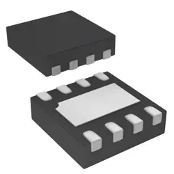
Images are for reference only
74AVC1T45GM
Nexperia
- Manufacturer
- Mfr. Part #74AVC1T45GM
- Package
- Datasheet
- In Stock20407
100% Original & New
24 Hours ready to ship
365 Days Warranty
RFQ & Get more Discounts
Specifications
Overview
Description
Key features include low power consumption, fast switching speeds, and a wide range of applications in level translation for I/O ports, microcontrollers, and other digital devices. The 74AVC1T45GM is particularly useful in battery-powered applications due to its low quiescent current and small package size. It ensures reliable data transfer while minimizing the risk of damage to sensitive components by providing a safe voltage interface.
Overall, the 74AVC1T45GM is an essential component for modern electronic designs requiring voltage level shifting, enabling seamless communication across different logic levels.
Features
1. Voltage Compatibility: It supports operation from 1.2V to 3.6V, allowing for level shifting between different voltage domains.
2. Directionality: The device facilitates bidirectional data transfer, making it suitable for interfacing between different voltage levels without additional components.
3. High Speed: The 74AVC1T45GM offers fast switching speeds, enabling efficient data transmission in high-speed applications.
4. Low Static Power Consumption: It has minimal static power draw, which is beneficial for battery-powered devices.
5. Compact Package: Available in a small footprint, making it ideal for space-constrained designs.
6. Input/Output Compatibility: It is compatible with various logic families, ensuring versatility in designs.
Overall, the 74AVC1T45GM is well-suited for applications requiring reliable level shifting in mobile devices, microcontrollers, and other digital circuit integrations.
Package
Pinout
1. VCCA (Pin 1): Positive supply voltage for the A side (logic level).
2. A (Pin 2): Input/Output for the A side.
3. GND (Pin 3): Ground reference for the device.
4. GND (Pin 4): Ground reference for the device.
5. B (Pin 5): Input/Output for the B side.
6. VCCB (Pin 6): Positive supply voltage for the B side (logic level).
7. DIR (Pin 7): Direction control pin; determines the direction of data flow between A and B.
8. OE (Pin 8): Output enable pin; when LOW, allows data flow; when HIGH, disables outputs.
The device supports level shifting between different voltage domains, making it suitable for interfacing between devices operating at different voltage levels.
Manufacturer
Application
Equivalent
- 74LVC1T45 (low voltage)
- 74LVC1T66 (with additional features)
- TXB0101 (for bidirectional level shifting)
Ensure compatibility with voltage levels and specific application requirements when considering alternatives.
Shipping
Shipping MethodsWe
offer global shipping services through DHL, FedEx, TNT, UPS, or any other forwarder of your choice.
Shipping Fee Reference (DHL/FedEx):
DHL: Shipping cost ranges from $25-$45 (0.5kg), with an estimated delivery time of 2-5 business days.
FedEx: Shipping cost ranges from $25-$40 (0.5kg), with an estimated delivery time of 3-7 business days.
UPS: Shipping cost ranges from $25-$45 (0.5kg), with an estimated delivery time of 3-7 business days.
TNT: Shipping cost ranges from $25-$65 (0.5kg), with an estimated delivery time of 3-7 business days.
EMS: Shipping cost ranges from $30-$50 (0.5kg), with an estimated delivery time of 7-15 business days.
Registered Air Mail: Shipping cost is $2-$4 (0.1kg), with an estimated delivery time of 5-20 business days.
Payments
Payment Methods
The Payment term is 100% Prepaid.
Currently, we only accept the below payment methods:
1. PayPal
2. Credit/ Debit Card
3. Wire Transfer
Similar
-
![MX25L3233FM1I-08Q]() MX25L3233FM1I-08Q
MX25L3233FM1I-08Q
Macronix
-
![MX29F400CBTI-70G]() MX29F400CBTI-70G
MX29F400CBTI-70G
Macronix
-
![MX25V5126FM1I]() MX25V5126FM1I
MX25V5126FM1I
Macronix
-
![MX25V2033FM1I]() MX25V2033FM1I
MX25V2033FM1I
Macronix
-
![MX25L25673GMI-10G]() MX25L25673GMI-10G
MX25L25673GMI-10G
Macronix
-
![MX25U51279GXDR00]() MX25U51279GXDR00
MX25U51279GXDR00
Macronix
-
![MX25V1635FM2I]() MX25V1635FM2I
MX25V1635FM2I
Macronix
-
![MX25U3232FZBI02]() MX25U3232FZBI02
MX25U3232FZBI02
Macronix
-
![MX25L12833FZNI-10G]() MX25L12833FZNI-10..
MX25L12833FZNI-10..
Macronix
-
![MX29F800CBTI-70G]() MX29F800CBTI-70G
MX29F800CBTI-70G
Macronix
-
![MX29LV640ETTI-70G]() MX29LV640ETTI-70G
MX29LV640ETTI-70G
Macronix
-
![MX25U51245GZ4I00]() MX25U51245GZ4I00
MX25U51245GZ4I00
Macronix