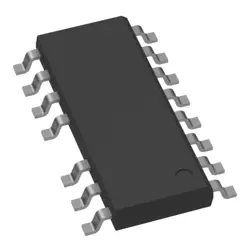
Images are for reference only
74HCT165D
Counter Shift Registers 8BIT SHIFT REGISTER PAR-IN/SERIAL-OUT
- Manufacturer
- Mfr. Part #74HCT165D
- Package
- Datasheet
- In Stock28501
100% Original & New
24 Hours ready to ship
365 Days Warranty
RFQ & Get more Discounts
Specifications
| Standard Pack Qty | 50 |
Overview
Description
Key features include a maximum clock frequency of 30 MHz, low power consumption, and compatibility with TTL logic levels due to its HCT (High-speed CMOS with TTL compatibility) design. It operates with a supply voltage range of 2V to 6V and has a simple interface, making it easy to integrate into various digital systems.
The 74HCT165D also supports cascading, allowing multiple shift registers to be connected to increase the number of outputs. It includes pins for clocking, enabling the shifting of data on each clock cycle, and a latch function to hold the output state. Overall, the 74HCT165D is a versatile component for digital signal processing and control applications.
Features
1. Functionality: It captures and shifts data serially and outputs it in parallel form.
2. Input/Output: It has 8 parallel output pins (Q0 to Q7) and a serial data input (DS).
3. Clock Control: Operates on a clock signal, transferring data on the rising edge.
4. Control Pins: Includes a shift/load control pin (SH/LD) for selecting between shifting data or loading it from the parallel inputs.
5. Reset Function: A reset pin (MR) initializes the outputs to low state.
6. TTL Compatibility: Designed to be compatible with TTL logic levels, making it suitable for integration in digital circuits.
7. High-Speed Operation: Capable of operating at clock speeds up to 25 MHz.
8. Power Supply: Operates with a supply voltage range of 4.5V to 5.5V.
These features make the 74HCT165D useful in applications such as data storage, signal processing, and digital circuit design.
Package
Pinout
1. Pin 1 (Q7): Serial output.
2. Pin 2 (Q6): Bit 6 output.
3. Pin 3 (Q5): Bit 5 output.
4. Pin 4 (Q4): Bit 4 output.
5. Pin 5 (Q3): Bit 3 output.
6. Pin 6 (Q2): Bit 2 output.
7. Pin 7 (Q1): Bit 1 output.
8. Pin 8 (Q0): Bit 0 output.
9. Pin 9 (GND): Ground.
10. Pin 10 (CLK): Shift register clock input.
11. Pin 11 (RCLK): Register clock input for output latches.
12. Pin 12 (SER): Serial data input.
13. Pin 13 (PL): Parallel load input (active low).
14. Pin 14 (MR): Master reset (active low).
15. Pin 15 (VCC): Power supply (usually +2V to +6V).
16. Pin 16 (Q7'): Optional inverted output.
This device is commonly used in digital electronics for data storage and manipulation.
Manufacturer
Application
Equivalent
- 74HC165
- 74LS165
- 74HCT595 (for similar applications, but with different functions)
Ensure to check specifications like voltage levels, package types, and pin configurations for compatibility.
Shipping
Shipping MethodsWe
offer global shipping services through DHL, FedEx, TNT, UPS, or any other forwarder of your choice.
Shipping Fee Reference (DHL/FedEx):
DHL: Shipping cost ranges from $25-$45 (0.5kg), with an estimated delivery time of 2-5 business days.
FedEx: Shipping cost ranges from $25-$40 (0.5kg), with an estimated delivery time of 3-7 business days.
UPS: Shipping cost ranges from $25-$45 (0.5kg), with an estimated delivery time of 3-7 business days.
TNT: Shipping cost ranges from $25-$65 (0.5kg), with an estimated delivery time of 3-7 business days.
EMS: Shipping cost ranges from $30-$50 (0.5kg), with an estimated delivery time of 7-15 business days.
Registered Air Mail: Shipping cost is $2-$4 (0.1kg), with an estimated delivery time of 5-20 business days.
Payments
Payment Methods
The Payment term is 100% Prepaid.
Currently, we only accept the below payment methods:
1. PayPal
2. Credit/ Debit Card
3. Wire Transfer
Similar
-
![MX25L3233FZBI-08Q]() MX25L3233FZBI-08Q
Macronix
-
![MX25V1635FZNQ03]() MX25V1635FZNQ03
Macronix
-
![MX25V4035FZUI]() MX25V4035FZUI
Macronix
-
![MX25V16066M1I02]() MX25V16066M1I02
Macronix
-
![MX25V16066M2I02]() MX25V16066M2I02
Macronix
-
![MX25R6435FBDIL0]() MX25R6435FBDIL0
Macronix
-
![MX29GL512FHXFI-11G]() MX29GL512FHXFI-11..
Macronix
-
![MX25U51279GXDR00]() MX25U51279GXDR00
Macronix
-
![MX25V1635FM2I]() MX25V1635FM2I
Macronix
-
![MX25U25645GXDI00]() MX25U25645GXDI00
Macronix
-
![MX25L25645GXDI-08G]() MX25L25645GXDI-08..
Macronix
-
![MX25L25735FMI-10G]() MX25L25735FMI-10G
Macronix