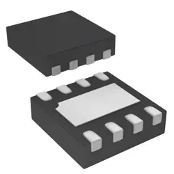
Images are for reference only
74HCT3G34DC
Nexperia
- Manufacturer
- Mfr. Part #74HCT3G34DC
- Package
- Datasheet
- In Stock26362
100% Original & New
24 Hours ready to ship
365 Days Warranty
RFQ & Get more Discounts
Specifications
Overview
Description
Operating at a wide voltage range from 2V to 5.5V, the 74HCT3G34DC is optimized for low power consumption, reducing heat generation and extending battery life in portable applications. Its small package size (often available in a SOT-23 or similar) makes it ideal for space-constrained designs. The device operates with a fast switching speed, suitable for high-frequency applications.
Common applications include signal buffering, level shifting, and driving LED displays in consumer electronics and industrial automation systems. Overall, the 74HCT3G34DC is a versatile component in modern digital circuit designs.
Features
1. Triple Buffers: It contains three independent buffers, allowing it to drive multiple loads in digital systems.
2. High-Speed Operation: Designed for fast switching, suitable for high-speed applications.
3. Low Power Consumption: Operates at low voltage levels while maintaining high performance, making it energy-efficient.
4. Wide Supply Voltage Range: Compatible with a supply voltage range of 2V to 5.5V.
5. TTL Compatibility: The HCT family is compatible with TTL (Transistor-Transistor Logic) levels.
6. Output Drive Capability: Capable of driving a standard load, making it suitable for interfacing with various devices.
7. Wide Temperature Range: Suitable for use in varying environmental conditions.
8. Small Package Size: Available in a compact package, aiding in space-constrained designs.
The 74HCT3G34DC is ideal for applications requiring reliable signal buffering and driving capabilities in digital systems.
Package
Pinout
The pinout is as follows:
- Pins 1, 2: Inputs A and B for the first NAND gate
- Pin 3: Output Y for the first NAND gate
- Pins 4, 5: Inputs A and B for the second NAND gate
- Pin 6: Output Y for the second NAND gate
- Pins 7, 8: Inputs A and B for the third NAND gate
- Pin 9: Output Y for the third NAND gate
- Pins 10, 11: Inputs A and B for the fourth NAND gate
- Pin 12: Output Y for the fourth NAND gate
- Pin 13: Ground (GND)
- Pin 14: VCC (Positive supply voltage)
The 74HCT3G34DC operates with a logic level compatible with TTL (Transistor-Transistor Logic) and is used for various digital logic applications.
Manufacturer
Application
Equivalent
Shipping
Shipping MethodsWe
offer global shipping services through DHL, FedEx, TNT, UPS, or any other forwarder of your choice.
Shipping Fee Reference (DHL/FedEx):
DHL: Shipping cost ranges from $25-$45 (0.5kg), with an estimated delivery time of 2-5 business days.
FedEx: Shipping cost ranges from $25-$40 (0.5kg), with an estimated delivery time of 3-7 business days.
UPS: Shipping cost ranges from $25-$45 (0.5kg), with an estimated delivery time of 3-7 business days.
TNT: Shipping cost ranges from $25-$65 (0.5kg), with an estimated delivery time of 3-7 business days.
EMS: Shipping cost ranges from $30-$50 (0.5kg), with an estimated delivery time of 7-15 business days.
Registered Air Mail: Shipping cost is $2-$4 (0.1kg), with an estimated delivery time of 5-20 business days.
Payments
Payment Methods
The Payment term is 100% Prepaid.
Currently, we only accept the below payment methods:
1. PayPal
2. Credit/ Debit Card
3. Wire Transfer
Similar
-
![MX25V1635FZNQ03]() MX25V1635FZNQ03
MX25V1635FZNQ03
Macronix
-
![MX66U1G45GXDI00]() MX66U1G45GXDI00
MX66U1G45GXDI00
Macronix
-
![MX25R6435FBDIL0]() MX25R6435FBDIL0
MX25R6435FBDIL0
Macronix
-
![MX25U51279GXDR00]() MX25U51279GXDR00
MX25U51279GXDR00
Macronix
-
![MX25U25643GZNI00]() MX25U25643GZNI00
MX25U25643GZNI00
Macronix
-
![MX25L2006EM1I-12G]() MX25L2006EM1I-12G
MX25L2006EM1I-12G
Macronix
-
![MX25R1635FZUIH0]() MX25R1635FZUIH0
MX25R1635FZUIH0
Macronix
-
![MX25U3232FZBI02]() MX25U3232FZBI02
MX25U3232FZBI02
Macronix
-
![MX25L6433FM2I-08G]() MX25L6433FM2I-08G
MX25L6433FM2I-08G
Macronix
-
![MX25U25645GXDI00]() MX25U25645GXDI00
MX25U25645GXDI00
Macronix
-
![MX29LV160DTTI-70G]() MX29LV160DTTI-70G
MX29LV160DTTI-70G
Macronix
-
![MX29F040CTI-70G]() MX29F040CTI-70G
MX29F040CTI-70G
Macronix