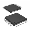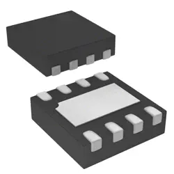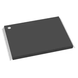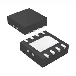

Images are for reference only
74LVC07AD
Buffers & Line Drivers HEX BUFFER/DRIVER
- Manufacturer
- Mfr. Part #74LVC07AD
- Package
- Datasheet
- In Stock28882
100% Original & New
24 Hours ready to ship
365 Days Warranty
RFQ & Get more Discounts
Specifications
| Standard Pack Qty | 57 |
Overview
Description
Key features include CMOS technology, allowing for low static power dissipation, and three-state outputs that can be easily enabled or disabled, facilitating bus-oriented systems. The 74LVC07AD can accept input voltages as low as 0.8V for a high signal, making it compatible with various logic levels.
Typical applications include signal buffering in data communications, interfacing between different logic families, and enhancing drive capability for LEDs or other loads. The device is available in various packages, making it versatile for different PCB designs. Overall, the 74LVC07AD is a reliable choice for applications requiring robust signal buffering and low power usage.
Features
1. Logic Levels: Compatible with both TTL and CMOS logic levels, operating at a supply voltage range of 1.65V to 5.5V.
2. Output Drive Capability: Provides strong output drive (up to 24mA) with high-speed performance.
3. Three-State Outputs: Each of the six outputs can be enabled or disabled, allowing for easy interfacing with other digital circuits.
4. Low Power Consumption: Designed for low-power applications, making it suitable for battery-operated devices.
5. Wide Operating Temperature: Supports a temperature range from -40°C to +85°C, ensuring reliability in various environments.
6. Bus Compatibility: Ideal for driving capacitive loads and interfacing with various bus systems.
7. Pin Configuration: Available in multiple package types (such as TSSOP and SOIC) for flexible design options.
Overall, the 74LVC07AD is versatile for use in digital signal buffering and level shifting applications.
Package
Pinout
- Pins 1, 3, 5, 7, 9, 11 (1A to 6A): Inputs for the six buffers.
- Pins 2, 4, 6, 8, 10, 12 (1Y to 6Y): Open-collector outputs corresponding to the inputs.
- Pin 13 (GND): Ground connection.
- Pin 14 (VCC): Power supply connection.
The open-collector outputs allow for wired-AND configuration with pull-up resistors, enabling multiple outputs to be connected to a common line. The device is typically used in digital circuits for signal buffering and driving higher loads.
Manufacturer
Application
Equivalent
1. 74LVC07A - Similar functionality without the "D" package designation.
2. 74LVC07APW - Same functionality in a TSSOP package.
3. 74HCT07 - High-speed CMOS version, compatible with TTL levels.
Always verify pin configuration and electrical characteristics to ensure compatibility for your application.
Shipping
Shipping MethodsWe
offer global shipping services through DHL, FedEx, TNT, UPS, or any other forwarder of your choice.
Shipping Fee Reference (DHL/FedEx):
DHL: Shipping cost ranges from $25-$45 (0.5kg), with an estimated delivery time of 2-5 business days.
FedEx: Shipping cost ranges from $25-$40 (0.5kg), with an estimated delivery time of 3-7 business days.
UPS: Shipping cost ranges from $25-$45 (0.5kg), with an estimated delivery time of 3-7 business days.
TNT: Shipping cost ranges from $25-$65 (0.5kg), with an estimated delivery time of 3-7 business days.
EMS: Shipping cost ranges from $30-$50 (0.5kg), with an estimated delivery time of 7-15 business days.
Registered Air Mail: Shipping cost is $2-$4 (0.1kg), with an estimated delivery time of 5-20 business days.
Payments
Payment Methods
The Payment term is 100% Prepaid.
Currently, we only accept the below payment methods:
1. PayPal
2. Credit/ Debit Card
3. Wire Transfer
Similar
-
![MX25L3233FM1I-08Q]() MX25L3233FM1I-08Q
Macronix
-
![MX66U1G45GXDI00]() MX66U1G45GXDI00
Macronix
-
![MX25V5126FM1I]() MX25V5126FM1I
Macronix
-
![MX25V16066M2I02]() MX25V16066M2I02
Macronix
-
![MX25L8035EM2I-10G]() MX25L8035EM2I-10G
Macronix
-
![MX25U25643GZNI00]() MX25U25643GZNI00
Macronix
-
![MX25R1635FZUIH0]() MX25R1635FZUIH0
Macronix
-
![MX25V1635FM2I]() MX25V1635FM2I
Macronix
-
![MX25L6433FM2I-08G]() MX25L6433FM2I-08G
Macronix
-
![MX29F800CBTI-70G]() MX29F800CBTI-70G
Macronix
-
![MX29LV640ETTI-70G]() MX29LV640ETTI-70G
Macronix
-
![MX25U51245GZ4I00]() MX25U51245GZ4I00
Macronix