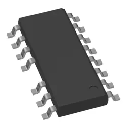
Images are for reference only
74LVC1G74GT
NOW NEXPERIA 74LVC1G74GT - D FLI
- Manufacturer
- Mfr. Part #74LVC1G74GT
- Package DFN8
- Datasheet 74LVC1G74GT DataSheet
- In Stock4540
100% Original & New
24 Hours ready to ship
365 Days Warranty
RFQ & Get more Discounts
Specifications
| Package | Bulk |
| ProductStatus | Active |
Overview
Description
Key features include:
- Single Flip-Flop Design: Allows for compact integration in various applications.
- Low Voltage Operation: Compatible with modern low-voltage logic levels.
- High Speed: Capable of switching at high frequencies, enhancing performance in fast circuits.
- High Noise Immunity: Ensures reliable operation in noisy environments.
- Wide Operating Temperature: Suitable for industrial applications.
Applications include data storage, frequency division, and state retention in digital systems. The 74LVC1G74GT is ideal for designs requiring efficient power management and reliable data handling.
Features
1. Input Voltage Range: Operates from 1.65V to 5.5V, making it suitable for modern low-power designs.
2. High Speed: Typical propagation delay of 5ns at 3.3V, ensuring fast switching performance.
3. Low Power Consumption: Consumes minimal static and dynamic power, ideal for battery-operated devices.
4. Asynchronous Reset: Features an active-low reset pin for immediate state control.
5. Single Flip-Flop Configuration: Compact design for space-constrained applications.
6. Wide Operating Temperature: Functions reliably in the -40°C to +125°C range.
7. TTL Compatibility: Compatible with both TTL and CMOS logic levels, allowing for versatile interfacing.
8. Small Package Options: Available in various packages, including SC70 and SOT-23, facilitating integration in dense layouts.
These features make the 74LVC1G74GT suitable for use in telecommunications, automotive, and consumer electronics applications.
Package
Pinout
### Pin Functions:
1. VCC: Power supply pin (typically +3.3V).
2. GND: Ground pin.
3. D: Data input pin where the data to be stored is applied.
4. CLK: Clock input pin that triggers the flip-flop to capture the value present at the D input on the rising edge of the clock signal.
5. Q: Output pin that reflects the stored value of the D input after the clock pulse.
This flip-flop is part of the LVC family, known for low-voltage and low-power operation, and it provides better performance in high-speed applications. The device is typically used in digital circuits for data storage and transfer.
Manufacturer
Application
Equivalent
Shipping
Shipping MethodsWe
offer global shipping services through DHL, FedEx, TNT, UPS, or any other forwarder of your choice.
Shipping Fee Reference (DHL/FedEx):
DHL: Shipping cost ranges from $25-$45 (0.5kg), with an estimated delivery time of 2-5 business days.
FedEx: Shipping cost ranges from $25-$40 (0.5kg), with an estimated delivery time of 3-7 business days.
UPS: Shipping cost ranges from $25-$45 (0.5kg), with an estimated delivery time of 3-7 business days.
TNT: Shipping cost ranges from $25-$65 (0.5kg), with an estimated delivery time of 3-7 business days.
EMS: Shipping cost ranges from $30-$50 (0.5kg), with an estimated delivery time of 7-15 business days.
Registered Air Mail: Shipping cost is $2-$4 (0.1kg), with an estimated delivery time of 5-20 business days.
Payments
Payment Methods
The Payment term is 100% Prepaid.
Currently, we only accept the below payment methods:
1. PayPal
2. Credit/ Debit Card
3. Wire Transfer
Similar
-
![MX25V1635FZNI]() MX25V1635FZNI
MX25V1635FZNI
Macronix
-
![MX25V1635FZNQ03]() MX25V1635FZNQ03
MX25V1635FZNQ03
Macronix
-
![MX25V2033FM1I]() MX25V2033FM1I
MX25V2033FM1I
Macronix
-
![MX25R6435FBDIL0]() MX25R6435FBDIL0
MX25R6435FBDIL0
Macronix
-
![MX29GL512FHXFI-11G]() MX29GL512FHXFI-11..
MX29GL512FHXFI-11..
Macronix
-
![MX25L2006EM1I-12G]() MX25L2006EM1I-12G
MX25L2006EM1I-12G
Macronix
-
![MX25L6433FM2I-08G]() MX25L6433FM2I-08G
MX25L6433FM2I-08G
Macronix
-
![MX25U6435FM2I-10G]() MX25U6435FM2I-10G
MX25U6435FM2I-10G
Macronix
-
![MX25L12833FM2I-10G]() MX25L12833FM2I-10..
MX25L12833FM2I-10..
Macronix
-
![MX29F800CBTI-70G]() MX29F800CBTI-70G
MX29F800CBTI-70G
Macronix
-
![MX25L25735FMI-10G]() MX25L25735FMI-10G
MX25L25735FMI-10G
Macronix
-
![MX30LF4G18AC-TI]() MX30LF4G18AC-TI
MX30LF4G18AC-TI
Macronix