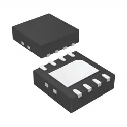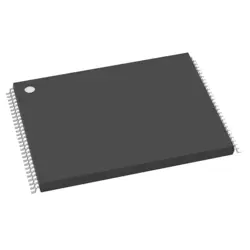
Images are for reference only
74LVT125PW
- Manufacturer
- Mfr. Part #74LVT125PW
- Package
- Datasheet
- In Stock9040
100% Original & New
24 Hours ready to ship
365 Days Warranty
RFQ & Get more Discounts
Specifications
| Brand | Nexperia |
| Product Type | Buffers & Line Drivers |
| Subcategory | Logic ICs |
| Logic Family | LVT |
Overview
Description
Key features include low power consumption, high output drive capability, and tri-state outputs, allowing for easy interfacing with other devices. The 74LVT125PW is housed in a 14-pin TSSOP package, which offers a compact footprint for space-constrained designs. It is commonly used in applications such as data buses, signal buffering, and level shifting.
Overall, the 74LVT125PW is an essential component for engineers looking to implement reliable and efficient signal management in their electronic designs.
Features
1. Low Voltage Operation: It operates at a supply voltage range of 1.65V to 3.6V, making it suitable for low-power applications.
2. High Speed: The device offers fast switching times, enhancing performance in high-speed digital circuits.
3. Three-State Outputs: Each of the four buffers can independently drive loads and go into a high-impedance state, allowing for bus-oriented applications.
4. TTL Compatibility: It is compatible with TTL levels, which ensures interoperability with other logic families.
5. Low Power Consumption: The device has low static and dynamic power usage, making it efficient for battery-powered applications.
6. Wide Operating Temperature: It can operate in a temperature range of -40°C to +125°C, suitable for various environmental conditions.
7. DIP and SOIC Packages: Available in multiple package types, including DIP and SOIC, for versatile design options.
These features make the 74LVT125PW ideal for data buffering and signal driving applications in modern electronic systems.
Package
Pinout
### Pin Configuration:
1. GND (Pin 1): Ground
2. 1A (Pin 2): Input for buffer 1
3. 1Y (Pin 3): Output for buffer 1
4. 1OE (Pin 4): Output Enable for buffer 1
5. 2A (Pin 5): Input for buffer 2
6. 2Y (Pin 6): Output for buffer 2
7. 2OE (Pin 7): Output Enable for buffer 2
8. GND (Pin 8): Ground
9. 3A (Pin 9): Input for buffer 3
10. 3Y (Pin 10): Output for buffer 3
11. 3OE (Pin 11): Output Enable for buffer 3
12. 4A (Pin 12): Input for buffer 4
13. 4Y (Pin 13): Output for buffer 4
14. 4OE (Pin 14): Output Enable for buffer 4
15. VCC (Pin 15): Positive power supply
16. NC (Pin 16): No Connect
This IC operates with a wide voltage range and is commonly used in applications needing buffering for high-speed data transmission.
Manufacturer
Application
Equivalent
Shipping
Shipping MethodsWe
offer global shipping services through DHL, FedEx, TNT, UPS, or any other forwarder of your choice.
Shipping Fee Reference (DHL/FedEx):
DHL: Shipping cost ranges from $25-$45 (0.5kg), with an estimated delivery time of 2-5 business days.
FedEx: Shipping cost ranges from $25-$40 (0.5kg), with an estimated delivery time of 3-7 business days.
UPS: Shipping cost ranges from $25-$45 (0.5kg), with an estimated delivery time of 3-7 business days.
TNT: Shipping cost ranges from $25-$65 (0.5kg), with an estimated delivery time of 3-7 business days.
EMS: Shipping cost ranges from $30-$50 (0.5kg), with an estimated delivery time of 7-15 business days.
Registered Air Mail: Shipping cost is $2-$4 (0.1kg), with an estimated delivery time of 5-20 business days.
Payments
Payment Methods
The Payment term is 100% Prepaid.
Currently, we only accept the below payment methods:
1. PayPal
2. Credit/ Debit Card
3. Wire Transfer
Similar
-
![MX66U1G45GXDI00]() MX66U1G45GXDI00
Macronix
-
![MX25V16066M2I02]() MX25V16066M2I02
Macronix
-
![MX25L25673GMI-10G]() MX25L25673GMI-10G
Macronix
-
![MX25U51279GXDR00]() MX25U51279GXDR00
Macronix
-
![MX25U25643GZNI00]() MX25U25643GZNI00
Macronix
-
![MX25L2006EM1I-12G]() MX25L2006EM1I-12G
Macronix
-
![MX25L12833FM2I-10G]() MX25L12833FM2I-10..
Macronix
-
![MX25L12833FZNI-10G]() MX25L12833FZNI-10..
Macronix
-
![MX25U25645GXDI00]() MX25U25645GXDI00
Macronix
-
![MX29LV160DTTI-70G]() MX29LV160DTTI-70G
Macronix
-
![MX25L25645GXDI-08G]() MX25L25645GXDI-08..
Macronix
-
![MX29F800CBTI-70G]() MX29F800CBTI-70G
Macronix