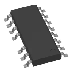
Images are for reference only
74LVX125MTCX
IC BUF NON-INVERT 3.6V 14TSSOP
- Manufacturer
- Mfr. Part #74LVX125MTCX
- Package TSSOP-14
- Datasheet 74LVX125MTCX DataSheet
- In Stock7560
100% Original & New
24 Hours ready to ship
365 Days Warranty
RFQ & Get more Discounts
Specifications
| Package | Bulk |
| Series | 74LVX |
| ProductStatus | Active |
| LogicType | Buffer, Non-Inverting |
| NumberofElements | 4 |
| NumberofBitsperElement | 1 |
| OutputType | 3-State |
| Current-OutputHighLow | 4mA, 4mA |
| Voltage-Supply | 2V ~ 3.6V |
| OperatingTemperature | -40°C ~ 85°C (TA) |
| MountingType | Surface Mount |
| Package/Case | 14-TSSOP (0.173, 4.40mm Width) |
Overview
Description
Key characteristics include a wide supply voltage range (2V to 5.5V), high output drive current (up to 24mA), and fast propagation delays (typically around 4ns at 5V). The 74LVX125 is commonly used in applications such as signal buffering, level shifting, and data routing in digital circuits. Its small package size (TSSOP or equivalent) makes it suitable for space-constrained environments. Overall, the 74LVX125MTCX provides a reliable solution for enhancing signal integrity in modern electronic designs.
Features
- Quad Configuration: Contains four independent buffers/drivers.
- 3-State Outputs: Each output can be enabled or disabled, allowing for bus interfacing.
- Low Voltage Operation: Designed to operate from a supply voltage of 1.2V to 5.5V, suitable for low-power applications.
- High Speed: Offers fast switching times, enhancing performance in high-speed data transmission.
- Low Power Consumption: Consumes minimal power, making it ideal for battery-operated devices.
- TTL Compatible: Compatible with TTL logic levels, allows integration with various logic families.
- Wide Operating Temperature Range: Functions reliably within a temperature range of -40°C to +125°C.
- Small Package: Available in a compact TSSOP package, facilitating space-efficient PCB designs.
Overall, the 74LVX125MTCX is suitable for applications requiring signal buffering, driving capabilities, and high-speed operation in low-voltage environments.
Package
Pinout
Pin Functions:
- 1, 2, 3, 4 (A1, A2, A3, A4): Inputs for the buffer/driver.
- 5, 6, 7, 8 (Y1, Y2, Y3, Y4): Outputs corresponding to each input.
- 9 (GND): Ground connection.
- 10 (VCC): Power supply connection.
- 11, 12, 13, 14 (OE1, OE2, OE3, OE4): Output enable inputs for tri-state control.
- 15, 16: Unused or NC (not connected).
- 17-20: Additional pins for input/output functions, depending on the specific configuration.
This device is commonly used in data communications and other applications requiring signal buffering.
Manufacturer
Application
Equivalent
Shipping
Shipping MethodsWe
offer global shipping services through DHL, FedEx, TNT, UPS, or any other forwarder of your choice.
Shipping Fee Reference (DHL/FedEx):
DHL: Shipping cost ranges from $25-$45 (0.5kg), with an estimated delivery time of 2-5 business days.
FedEx: Shipping cost ranges from $25-$40 (0.5kg), with an estimated delivery time of 3-7 business days.
UPS: Shipping cost ranges from $25-$45 (0.5kg), with an estimated delivery time of 3-7 business days.
TNT: Shipping cost ranges from $25-$65 (0.5kg), with an estimated delivery time of 3-7 business days.
EMS: Shipping cost ranges from $30-$50 (0.5kg), with an estimated delivery time of 7-15 business days.
Registered Air Mail: Shipping cost is $2-$4 (0.1kg), with an estimated delivery time of 5-20 business days.
Payments
Payment Methods
The Payment term is 100% Prepaid.
Currently, we only accept the below payment methods:
1. PayPal
2. Credit/ Debit Card
3. Wire Transfer
Similar
-
![MX29F400CBTI-70G]() MX29F400CBTI-70G
MX29F400CBTI-70G
Macronix
-
![MX25V2033FM1I]() MX25V2033FM1I
MX25V2033FM1I
Macronix
-
![MX25V16066M1I02]() MX25V16066M1I02
MX25V16066M1I02
Macronix
-
![MX25L8035EM2I-10G]() MX25L8035EM2I-10G
MX25L8035EM2I-10G
Macronix
-
![MX25R6435FBDIL0]() MX25R6435FBDIL0
MX25R6435FBDIL0
Macronix
-
![MX25L25673GMI-08G]() MX25L25673GMI-08G
MX25L25673GMI-08G
Macronix
-
![MX25U51279GXDR00]() MX25U51279GXDR00
MX25U51279GXDR00
Macronix
-
![MX25L6433FM2I-08G]() MX25L6433FM2I-08G
MX25L6433FM2I-08G
Macronix
-
![MX29F800CBTI-70G]() MX29F800CBTI-70G
MX29F800CBTI-70G
Macronix
-
![MX29LV640ETTI-70G]() MX29LV640ETTI-70G
MX29LV640ETTI-70G
Macronix
-
![MX25L25735FMI-10G]() MX25L25735FMI-10G
MX25L25735FMI-10G
Macronix
-
![MX30LF4G18AC-TI]() MX30LF4G18AC-TI
MX30LF4G18AC-TI
Macronix