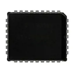
Images are for reference only
74VHC245PW
- Manufacturer
- Mfr. Part #74VHC245PW
- Package
- Datasheet
- In Stock8925
100% Original & New
24 Hours ready to ship
365 Days Warranty
RFQ & Get more Discounts
Specifications
| Brand | Nexperia |
Overview
Description
Key features of the 74VHC245PW include:
- Operating voltage range: 2.0V to 5.5V, making it suitable for both 3.3V and 5V systems.
- High-speed operation with typical propagation delay of around 5.5ns.
- Low static power consumption due to CMOS technology.
- Output capability of driving 15 LSTTL loads.
- 3-state outputs allowing bus connection and isolation.
- Direction and output enable controls for flexible data flow management.
This transceiver is typically housed in a TSSOP package, which is compact and suitable for densely packed PCBs. The 74VHC245PW is widely used in digital circuits where data needs to be transmitted between different parts of a system without interference, such as in microcontroller interfaces, memory systems, and data multiplexing applications.
Features
1. Octal Bus Transceiver: Facilitates communication between two separate data buses.
2. 3-State Outputs: Allows the outputs to be in a high-impedance state, enabling multiple transceivers to be connected to the same data lines.
3. TTL-Compatible Inputs: Ensures compatibility with TTL logic levels.
4. Low Power Consumption: Operates with minimal power usage, making it suitable for power-sensitive applications.
5. Wide Supply Voltage Range: Typically operates from 2.0V to 5.5V, offering flexibility in various applications.
6. High-Speed Operation: Provides fast data transfer rates, suitable for high-performance applications.
7. Latch-Up Performance: Offers good latch-up immunity with a high level of reliability.
8. Compact Package: Available in a TSSOP (Thin Shrink Small Outline Package), which saves space on circuit boards.
These features make the 74VHC245PW suitable for a variety of applications in computing, communications, and industrial systems.
Package
Pinout
- Pins 2-9 (A1-A8): Data inputs/outputs for Bus A.
- Pins 11-18 (B1-B8): Data inputs/outputs for Bus B.
- Pin 1 (DIR): Direction control. Determines the direction of data flow. When DIR is high, data flows from A to B. When DIR is low, data flows from B to A.
- Pin 19 (OE): Output enable. When OE is low, the device is enabled, and data can be transmitted. When OE is high, the outputs are in a high-impedance state.
- Pin 10 (GND): Ground connection.
- Pin 20 (VCC): Supply voltage.
This device is used for bus isolation, address multiplexing, and other applications requiring bidirectional data transfer with tri-state capability.
Manufacturer
Application
Equivalent
Shipping
Shipping MethodsWe
offer global shipping services through DHL, FedEx, TNT, UPS, or any other forwarder of your choice.
Shipping Fee Reference (DHL/FedEx):
DHL: Shipping cost ranges from $25-$45 (0.5kg), with an estimated delivery time of 2-5 business days.
FedEx: Shipping cost ranges from $25-$40 (0.5kg), with an estimated delivery time of 3-7 business days.
UPS: Shipping cost ranges from $25-$45 (0.5kg), with an estimated delivery time of 3-7 business days.
TNT: Shipping cost ranges from $25-$65 (0.5kg), with an estimated delivery time of 3-7 business days.
EMS: Shipping cost ranges from $30-$50 (0.5kg), with an estimated delivery time of 7-15 business days.
Registered Air Mail: Shipping cost is $2-$4 (0.1kg), with an estimated delivery time of 5-20 business days.
Payments
Payment Methods
The Payment term is 100% Prepaid.
Currently, we only accept the below payment methods:
1. PayPal
2. Credit/ Debit Card
3. Wire Transfer
Similar
-
![MX25L3233FM1I-08Q]() MX25L3233FM1I-08Q
MX25L3233FM1I-08Q
Macronix
-
![MX29F400CBTI-70G]() MX29F400CBTI-70G
MX29F400CBTI-70G
Macronix
-
![MX25R3235FZNIL0]() MX25R3235FZNIL0
MX25R3235FZNIL0
Macronix
-
![MX25L8035EM2I-10G]() MX25L8035EM2I-10G
MX25L8035EM2I-10G
Macronix
-
![MX25L25673GMI-10G]() MX25L25673GMI-10G
MX25L25673GMI-10G
Macronix
-
![MX29GL512FHXFI-11G]() MX29GL512FHXFI-11..
MX29GL512FHXFI-11..
Macronix
-
![MX25L12833FM2I-10G]() MX25L12833FM2I-10..
MX25L12833FM2I-10..
Macronix
-
![MX25L12833FZ2I-10G]() MX25L12833FZ2I-10..
MX25L12833FZ2I-10..
Macronix
-
![MX25L12835FZ2I-10G]() MX25L12835FZ2I-10..
MX25L12835FZ2I-10..
Macronix
-
![MX29F040CQI-70G]() MX29F040CQI-70G
MX29F040CQI-70G
Macronix
-
![MX29LV640ETTI-70G]() MX29LV640ETTI-70G
MX29LV640ETTI-70G
Macronix
-
![MX25L1006EMI-10G]() MX25L1006EMI-10G
MX25L1006EMI-10G
Macronix