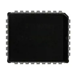
Images are for reference only
AD708JNZ
IC OPAMP GP 2 CIRCUIT 8DIP
- Manufacturer
- Mfr. Part #AD708JNZ
- Package PDIP-8
- Datasheet
- In Stock4500
100% Original & New
24 Hours ready to ship
365 Days Warranty
RFQ & Get more Discounts
Specifications
| Package | Tube |
| ProductStatus | Active |
| AmplifierType | General Purpose |
| NumberofCircuits | 2 |
| SlewRate | 0.3V/µs |
| GainBandwidthProduct | 900 kHz |
| -3dbBandwidth | 900 kHz |
| Current-InputBias | 1 nA |
| Voltage-InputOffset | 30 µV |
| Current-Supply | 4.5mA |
| Voltage-SupplySpan(Min) | 6 V |
| Voltage-SupplySpan(Max) | 36 V |
| OperatingTemperature | 0°C ~ 70°C |
| MountingType | Through Hole |
| Package/Case | 8-DIP (0.300, 7.62mm) |
Overview
Description
Key specifications of the AD708JNZ include a typical offset voltage of 50 µV, a noise density of 12 nV/√Hz, and a common-mode rejection ratio (CMRR) of 100 dB. It also has a wide bandwidth and fast slew rate, which enhance its performance in dynamic applications.
The AD708JNZ is available in various package options, making it versatile for integration into different designs. Its reliability and performance make it a popular choice in medical devices, industrial controls, and consumer electronics where signal integrity is critical.
Features
1. Low Offset Voltage: Typically 0.3 mV, ensuring accurate signal amplification.
2. Low Bias Current: Input bias current is around 4 nA, minimizing input error.
3. Wide Supply Voltage Range: Operates from ±2 V to ±18 V, providing versatility for various applications.
4. High Slew Rate: Typically 0.6 V/µs, allowing for rapid signal changes.
5. Low Noise: Voltage noise density is approximately 0.65 µV/√Hz at 1 kHz, making it suitable for sensitive applications.
6. High Open-Loop Gain: Provides a gain of 100 dB, enhancing signal fidelity.
7. Rail-to-Rail Output: Enables maximum output swing, suitable for single-supply operation.
These features make the AD708JNZ ideal for applications in instrumentation, data acquisition, and audio processing where precision and low distortion are critical.
Package
Pinout
Pinout Functions:
1. Pin 1 (Offset Null): Used for offset voltage adjustments.
2. Pin 2 (Inverting Input): The input for the inverting signal.
3. Pin 3 (Non-Inverting Input): The input for the non-inverting signal.
4. Pin 4 (V-): Negative power supply connection.
5. Pin 5 (Output): The output of the operational amplifier.
6. Pin 6 (V+): Positive power supply connection.
7. Pin 7 (Offset Null): Another pin for offset voltage adjustment.
8. Pin 8 (NC): No connection.
The AD708JNZ is designed for applications requiring low offset voltage, low noise, and high accuracy, making it suitable for sensor signal conditioning, instrumentation, and other precision analog tasks.
Manufacturer
Application
Equivalent
Shipping
Shipping MethodsWe
offer global shipping services through DHL, FedEx, TNT, UPS, or any other forwarder of your choice.
Shipping Fee Reference (DHL/FedEx):
DHL: Shipping cost ranges from $25-$45 (0.5kg), with an estimated delivery time of 2-5 business days.
FedEx: Shipping cost ranges from $25-$40 (0.5kg), with an estimated delivery time of 3-7 business days.
UPS: Shipping cost ranges from $25-$45 (0.5kg), with an estimated delivery time of 3-7 business days.
TNT: Shipping cost ranges from $25-$65 (0.5kg), with an estimated delivery time of 3-7 business days.
EMS: Shipping cost ranges from $30-$50 (0.5kg), with an estimated delivery time of 7-15 business days.
Registered Air Mail: Shipping cost is $2-$4 (0.1kg), with an estimated delivery time of 5-20 business days.
Payments
Payment Methods
The Payment term is 100% Prepaid.
Currently, we only accept the below payment methods:
1. PayPal
2. Credit/ Debit Card
3. Wire Transfer
Similar
-
![MX25L3233FZBI-08Q]() MX25L3233FZBI-08Q
Macronix
-
![MX25V4035FZUI]() MX25V4035FZUI
Macronix
-
![MX25V2033FM1I]() MX25V2033FM1I
Macronix
-
![MX25R6435FBDIL0]() MX25R6435FBDIL0
Macronix
-
![MX29GL512FHXFI-11G]() MX29GL512FHXFI-11..
Macronix
-
![MX25L2006EM1I-12G]() MX25L2006EM1I-12G
Macronix
-
![MX25V1635FM2I]() MX25V1635FM2I
Macronix
-
![MX25L12833FM2I-10G]() MX25L12833FM2I-10..
Macronix
-
![MX25L12833FZ2I-10G]() MX25L12833FZ2I-10..
Macronix
-
![MX25L12833FZNI-10G]() MX25L12833FZNI-10..
Macronix
-
![MX29LV160DTTI-70G]() MX29LV160DTTI-70G
Macronix
-
![MX29F040CQI-70G]() MX29F040CQI-70G
Macronix