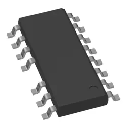
Images are for reference only
ADA4938-2ACPZ
ADI Dual Ultra-Low Distortion Diff ADC Drive
- Manufacturer
- Mfr. Part #ADA4938-2ACPZ
- Package
- Datasheet
- In Stock7793
100% Original & New
24 Hours ready to ship
365 Days Warranty
RFQ & Get more Discounts
Specifications
| Standard Pack Qty | 1500 |
Overview
Description
Key specifications include a typical input offset voltage of 0.1 mV, a gain bandwidth product of 12 MHz, and a low total harmonic distortion (THD). The device operates from a single or dual power supply, with a wide common-mode input voltage range, allowing for versatile integration into various systems.
The ADA4938-2ACPZ is available in a compact 8-lead LFCSP package, facilitating easy PCB design and space-saving applications. It's ideal for users needing precision signal amplification with minimal distortion and noise, enhancing overall system performance.
Features
1. High Speed: Offers a bandwidth of 200 MHz, making it suitable for high-frequency applications.
2. Low Noise: Maintains a low input voltage noise density of 1.2 nV/√Hz, which is crucial for sensitive signal processing.
3. Single-Supply Operation: Can operate with a single supply voltage ranging from 5V to 12V, enhancing versatility in design.
4. High Slew Rate: Features a slew rate of 2000 V/μs, allowing fast signal transitions.
5. Differential Inputs: Supports differential input signals, improving common-mode rejection and reducing noise.
6. Output Drive Capability: Capable of driving loads up to 600Ω while maintaining linearity.
7. Low Total Harmonic Distortion: THD is as low as -110 dB, ensuring high signal fidelity.
These attributes make the ADA4938-2ACPZ ideal for applications in communications, instrumentation, and medical devices.
Package
Pinout
1. Input Pins (IN+ and IN-): These are the differential input terminals for the signal.
2. Reference Pin (REF): This pin is used to set the output voltage reference level.
3. Gain Configuration Pins (RG1, RG2): These pins are used to set the gain of the amplifier.
4. Output Pins (OUT1 and OUT2): These provide the amplified output signals.
5. Power Supply Pins (V+ and V-): These are used to supply power to the amplifier.
6. Ground Pin (GND): This pin serves as the reference ground for the circuit.
7. Additional Functional Pins: These include shutdown and other control pins as needed for operation.
Overall, the device is designed for high-performance applications that require precise signal amplification.
Manufacturer
Application
Equivalent
Shipping
Shipping MethodsWe
offer global shipping services through DHL, FedEx, TNT, UPS, or any other forwarder of your choice.
Shipping Fee Reference (DHL/FedEx):
DHL: Shipping cost ranges from $25-$45 (0.5kg), with an estimated delivery time of 2-5 business days.
FedEx: Shipping cost ranges from $25-$40 (0.5kg), with an estimated delivery time of 3-7 business days.
UPS: Shipping cost ranges from $25-$45 (0.5kg), with an estimated delivery time of 3-7 business days.
TNT: Shipping cost ranges from $25-$65 (0.5kg), with an estimated delivery time of 3-7 business days.
EMS: Shipping cost ranges from $30-$50 (0.5kg), with an estimated delivery time of 7-15 business days.
Registered Air Mail: Shipping cost is $2-$4 (0.1kg), with an estimated delivery time of 5-20 business days.
Payments
Payment Methods
The Payment term is 100% Prepaid.
Currently, we only accept the below payment methods:
1. PayPal
2. Credit/ Debit Card
3. Wire Transfer
Similar
-
![MX25L3233FM1I-08Q]() MX25L3233FM1I-08Q
MX25L3233FM1I-08Q
Macronix
-
![MX25V2033FM1I]() MX25V2033FM1I
MX25V2033FM1I
Macronix
-
![MX25L8035EM2I-10G]() MX25L8035EM2I-10G
MX25L8035EM2I-10G
Macronix
-
![MX25U51279GXDR00]() MX25U51279GXDR00
MX25U51279GXDR00
Macronix
-
![MX25U25643GZNI00]() MX25U25643GZNI00
MX25U25643GZNI00
Macronix
-
![MX25L2006EM1I-12G]() MX25L2006EM1I-12G
MX25L2006EM1I-12G
Macronix
-
![MX25U6435FM2I-10G]() MX25U6435FM2I-10G
MX25U6435FM2I-10G
Macronix
-
![MX25U25645GXDI00]() MX25U25645GXDI00
MX25U25645GXDI00
Macronix
-
![MX25L25645GXDI-08G]() MX25L25645GXDI-08..
MX25L25645GXDI-08..
Macronix
-
![MX29F040CTI-70G]() MX29F040CTI-70G
MX29F040CTI-70G
Macronix
-
![MX25L25735FMI-10G]() MX25L25735FMI-10G
MX25L25735FMI-10G
Macronix
-
![MX25U51245GZ4I00]() MX25U51245GZ4I00
MX25U51245GZ4I00
Macronix