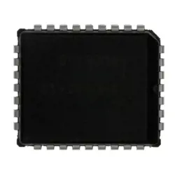
Images are for reference only
ADCLK905BCPZ
ADI 1:1 ECL, 7 Gbpps CLOCK/DATA BUFFERS
- Manufacturer
- Mfr. Part #ADCLK905BCPZ
- Package
- Datasheet
- In Stock16345
100% Original & New
24 Hours ready to ship
365 Days Warranty
RFQ & Get more Discounts
Specifications
| Standard Pack Qty | 50 |
Overview
Description
The device typically supports LVPECL and LVDS output formats, ensuring compatibility with a range of high-speed logic families. Its ability to drive multiple loads while maintaining signal integrity makes it suitable for communication systems, data converters, and networking equipment.
With a power supply range of 3.0V to 3.6V, the ADCLK905BCPZ also boasts low power consumption, making it efficient for power-sensitive applications. Additionally, it includes functionalities like enable/disable control, enhancing its versatility in various circuit configurations. Overall, the ADCLK905BCPZ is an essential component for engineers looking to improve the performance of timing signals in complex electronic systems.
Features
1. Low Jitter Performance: It offers low phase noise and jitter, making it suitable for high-speed data applications.
2. Wide Operating Frequency Range: Supports clock frequencies up to 1.5 GHz, accommodating various system requirements.
3. Multiple Outputs: Provides multiple low-skew outputs, ensuring synchronized clock signals across different components.
4. Integrated Voltage Level Shifting: Allows compatibility with various logic levels, enhancing design flexibility.
5. Power Supply Range: Operates from a single 3.3V power supply, simplifying power management.
6. Compact Package: Available in a 32-lead LFCSP package, enabling space-efficient designs.
7. Low Power Consumption: Designed for energy-efficient operation, suitable for portable applications.
These features make the ADCLK905BCPZ ideal for use in telecommunications, data communications, and high-speed digital systems.
Package
Pinout
The primary functions of the ADCLK905BCPZ include:
1. Clock Buffering: It provides multiple buffered outputs from a single input clock signal, which helps in driving high-capacitance loads.
2. Low Jitter Performance: The device is designed for low additive jitter, making it suitable for high-performance applications.
3. Output Control: The chip includes features for controlling the output enable/disable function.
4. Voltage Supply: It operates over a wide supply voltage range, typically from 2.5V to 3.3V.
The 16 pins serve various functions including power supply, ground, input clock, multiple output clocks, and control signals. For precise applications, refer to the specific datasheet for detailed pin assignments and functionalities.
Manufacturer
Application
Equivalent
Shipping
Shipping MethodsWe
offer global shipping services through DHL, FedEx, TNT, UPS, or any other forwarder of your choice.
Shipping Fee Reference (DHL/FedEx):
DHL: Shipping cost ranges from $25-$45 (0.5kg), with an estimated delivery time of 2-5 business days.
FedEx: Shipping cost ranges from $25-$40 (0.5kg), with an estimated delivery time of 3-7 business days.
UPS: Shipping cost ranges from $25-$45 (0.5kg), with an estimated delivery time of 3-7 business days.
TNT: Shipping cost ranges from $25-$65 (0.5kg), with an estimated delivery time of 3-7 business days.
EMS: Shipping cost ranges from $30-$50 (0.5kg), with an estimated delivery time of 7-15 business days.
Registered Air Mail: Shipping cost is $2-$4 (0.1kg), with an estimated delivery time of 5-20 business days.
Payments
Payment Methods
The Payment term is 100% Prepaid.
Currently, we only accept the below payment methods:
1. PayPal
2. Credit/ Debit Card
3. Wire Transfer
Similar
-
![MX25V1635FZNQ03]() MX25V1635FZNQ03
MX25V1635FZNQ03
Macronix
-
![MX25V2033FM1I]() MX25V2033FM1I
MX25V2033FM1I
Macronix
-
![MX25V16066M1I02]() MX25V16066M1I02
MX25V16066M1I02
Macronix
-
![MX25V16066M2I02]() MX25V16066M2I02
MX25V16066M2I02
Macronix
-
![MX29GL512FHXFI-11G]() MX29GL512FHXFI-11..
MX29GL512FHXFI-11..
Macronix
-
![MX25R1635FZUIH0]() MX25R1635FZUIH0
MX25R1635FZUIH0
Macronix
-
![MX25L12833FM2I-10G]() MX25L12833FM2I-10..
MX25L12833FM2I-10..
Macronix
-
![MX25U25645GXDI00]() MX25U25645GXDI00
MX25U25645GXDI00
Macronix
-
![MX29F040CQI-70G]() MX29F040CQI-70G
MX29F040CQI-70G
Macronix
-
![MX25L25645GXDI-08G]() MX25L25645GXDI-08..
MX25L25645GXDI-08..
Macronix
-
![MX29F040CTI-70G]() MX29F040CTI-70G
MX29F040CTI-70G
Macronix
-
![MX25L1006EMI-10G]() MX25L1006EMI-10G
MX25L1006EMI-10G
Macronix