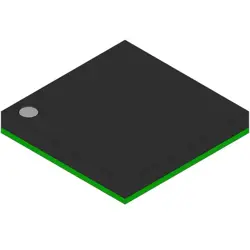
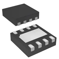
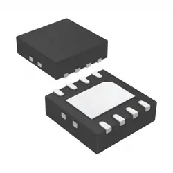
Images are for reference only
ADL5530ACPZ
- Manufacturer
- Mfr. Part #ADL5530ACPZ
- Package
- Datasheet
- In Stock2870
100% Original & New
24 Hours ready to ship
365 Days Warranty
RFQ & Get more Discounts
Specifications
| Brand | Analog Devices |
| Factory Pack Quantity:Factory Pack Quantity | 3000 |
Overview
Description
Key attributes include a supply voltage range of 4.5 V to 5.5 V and low power consumption, which enhances its suitability for portable applications. The ADL5530ACPZ utilizes a compact package design, facilitating easy integration into various systems. Additionally, it offers features like adjustable gain, enabling flexibility in diverse applications.
Overall, the ADL5530ACPZ is a versatile component that addresses the needs of modern RF signal processing, providing robust performance in a compact form factor.
Features
1. Wide Bandwidth: Operates effectively from DC to 1.0 GHz, making it suitable for RF and baseband applications.
2. Gain Control: Offers a programmable gain range of 0 to 31.5 dB with a 0.5 dB step size, allowing for fine adjustment.
3. Low Noise: Features a low noise figure (NF) of 1.2 dB at maximum gain, enhancing the signal-to-noise ratio.
4. High Linearity: Exhibits excellent linearity, making it ideal for applications that handle complex signals.
5. Single Supply Operation: Requires only a single supply voltage of 5V, simplifying design and integration.
6. Integrated Features: Includes a shutdown mode for power savings, and a low distortion characteristic for high-fidelity signal processing.
7. Temperature Range: Qualified for operation from -40°C to +85°C, suitable for industrial applications.
These features make the ADL5530ACPZ a versatile choice for communications, instrumentation, and imaging systems.
Package
Pinout
Key pins and their functions include:
1. RF Input (Pin 1 & Pin 2): For receiving RF signals.
2. RF Output (Pin 3): For outputting the amplified RF signal.
3. VDD (Pin 4 & Pin 5): Supply voltage inputs for powering the device.
4. GND (Pin 6 & Pin 7): Ground connections to provide a reference point.
5. Control Pins (like Pin 9 & Pin 10): Used for gain control and other adjustments.
6. Bypass Capacitor Pins (Pin 8, Pin 11): For stability and noise reduction.
7. NC (No Connect Pins, e.g., Pin 12): Not connected internally.
This amplifier is designed to operate over a wide frequency range, making it versatile for various RF applications.
Manufacturer
Application
Equivalent
Shipping
Shipping MethodsWe
offer global shipping services through DHL, FedEx, TNT, UPS, or any other forwarder of your choice.
Shipping Fee Reference (DHL/FedEx):
DHL: Shipping cost ranges from $25-$45 (0.5kg), with an estimated delivery time of 2-5 business days.
FedEx: Shipping cost ranges from $25-$40 (0.5kg), with an estimated delivery time of 3-7 business days.
UPS: Shipping cost ranges from $25-$45 (0.5kg), with an estimated delivery time of 3-7 business days.
TNT: Shipping cost ranges from $25-$65 (0.5kg), with an estimated delivery time of 3-7 business days.
EMS: Shipping cost ranges from $30-$50 (0.5kg), with an estimated delivery time of 7-15 business days.
Registered Air Mail: Shipping cost is $2-$4 (0.1kg), with an estimated delivery time of 5-20 business days.
Payments
Payment Methods
The Payment term is 100% Prepaid.
Currently, we only accept the below payment methods:
1. PayPal
2. Credit/ Debit Card
3. Wire Transfer
Similar
-
![MX25L3233FM1I-08Q]() MX25L3233FM1I-08Q
Macronix
-
![MX25V1635FZNI]() MX25V1635FZNI
Macronix
-
![MX25V4035FZUI]() MX25V4035FZUI
Macronix
-
![MX25L8035EM2I-10G]() MX25L8035EM2I-10G
Macronix
-
![MX25L25673GMI-08G]() MX25L25673GMI-08G
Macronix
-
![MX25L25673GMI-10G]() MX25L25673GMI-10G
Macronix
-
![MX29GL512FHXFI-11G]() MX29GL512FHXFI-11..
Macronix
-
![MX25R1635FZUIH0]() MX25R1635FZUIH0
Macronix
-
![MX25U6435FM2I-10G]() MX25U6435FM2I-10G
Macronix
-
![MX25L12833FM2I-10G]() MX25L12833FM2I-10..
Macronix
-
![MX25L12833FZNI-10G]() MX25L12833FZNI-10..
Macronix
-
![MX25L25645GXDI-08G]() MX25L25645GXDI-08..
Macronix