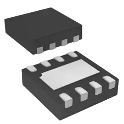
Images are for reference only
ADL5611ARKZ
ADI 2dB Noise Figure Gain Block
- Manufacturer
- Mfr. Part #ADL5611ARKZ
- Package
- Datasheet
- In Stock21349
100% Original & New
24 Hours ready to ship
365 Days Warranty
RFQ & Get more Discounts
Specifications
| Packaging | Reel |
| Standard Pack Qty | 1000 |
Overview
Description
Key features include excellent linearity, low power consumption, and a compact package size. The amplifier supports a wide supply voltage range, allowing versatility in various applications. Its design incorporates matched input and output impedance, simplifying integration with other RF components.
The ADL5611ARKZ is ideal for enhancing signal integrity in applications like 5G, satellite communications, and other high-frequency systems. Additionally, its low thermal resistance ensures reliable operation over a range of conditions, making it a robust choice for engineers looking to optimize performance in their RF designs.
Features
1. Wide Frequency Range: Operates from 1 MHz to 3 GHz, making it suitable for various RF and microwave applications.
2. High Gain: Provides a gain of up to 20 dB, enhancing signal levels for improved performance.
3. Low Noise Figure: Offers a low noise figure, typically around 2.4 dB, which improves receiver sensitivity.
4. Single Supply Operation: Can operate on a single supply voltage, typically from 3.0 to 5.5 volts, simplifying design.
5. High Linearity: Exhibits excellent linearity, minimizing distortion and maintaining signal integrity.
6. Compact Package: Available in a compact 8-lead LFCSP package, facilitating integration into space-constrained designs.
7. Temperature Range: Rated for operation over a -40°C to +85°C temperature range, ensuring reliability in various environments.
These features make the ADL5611ARKZ suitable for applications in wireless infrastructure, instrumentation, and commercial systems.
Package
Pinout
The pin functions are as follows:
1. RF Input: Input for the RF signal.
2. GND: Ground connection.
3. RF Output: Output for the amplified RF signal.
4. VCC: Supply voltage input.
5. VBIAS: Bias voltage input.
6. RFIN: RF input (can be used for matching network).
7. RFB: Feedback pin for external components.
8. VOUT: Output voltage pin for testing.
9. NC (Not Connected): No connection; can be left floating or connected to ground.
10. GND (second instance): Additional ground pin for improved thermal and electrical performance.
11. GND (third instance): Another ground pin to minimize potential ground loop issues.
12. VCC (second instance): Additional supply voltage pin for improved power distribution.
Each pin plays a crucial role in the amplifier's operation, ensuring optimal performance across a range of RF applications.
Manufacturer
Application
Equivalent
Shipping
Shipping MethodsWe
offer global shipping services through DHL, FedEx, TNT, UPS, or any other forwarder of your choice.
Shipping Fee Reference (DHL/FedEx):
DHL: Shipping cost ranges from $25-$45 (0.5kg), with an estimated delivery time of 2-5 business days.
FedEx: Shipping cost ranges from $25-$40 (0.5kg), with an estimated delivery time of 3-7 business days.
UPS: Shipping cost ranges from $25-$45 (0.5kg), with an estimated delivery time of 3-7 business days.
TNT: Shipping cost ranges from $25-$65 (0.5kg), with an estimated delivery time of 3-7 business days.
EMS: Shipping cost ranges from $30-$50 (0.5kg), with an estimated delivery time of 7-15 business days.
Registered Air Mail: Shipping cost is $2-$4 (0.1kg), with an estimated delivery time of 5-20 business days.
Payments
Payment Methods
The Payment term is 100% Prepaid.
Currently, we only accept the below payment methods:
1. PayPal
2. Credit/ Debit Card
3. Wire Transfer
Similar
-
![MX25R8035FM1IL0]() MX25R8035FM1IL0
MX25R8035FM1IL0
Macronix
-
![MX29F400CBTI-70G]() MX29F400CBTI-70G
MX29F400CBTI-70G
Macronix
-
![MX25V16066M1I02]() MX25V16066M1I02
MX25V16066M1I02
Macronix
-
![MX25R3235FZNIL0]() MX25R3235FZNIL0
MX25R3235FZNIL0
Macronix
-
![MX30LF2G28AD-TI]() MX30LF2G28AD-TI
MX30LF2G28AD-TI
Macronix
-
![MX25L25673GMI-10G]() MX25L25673GMI-10G
MX25L25673GMI-10G
Macronix
-
![MX25U25643GZNI00]() MX25U25643GZNI00
MX25U25643GZNI00
Macronix
-
![MX25L2006EM1I-12G]() MX25L2006EM1I-12G
MX25L2006EM1I-12G
Macronix
-
![MX25U3232FZBI02]() MX25U3232FZBI02
MX25U3232FZBI02
Macronix
-
![MX25L6433FM2I-08G]() MX25L6433FM2I-08G
MX25L6433FM2I-08G
Macronix
-
![MX25L12833FZ2I-10G]() MX25L12833FZ2I-10..
MX25L12833FZ2I-10..
Macronix
-
![MX29F040CTI-70G]() MX29F040CTI-70G
MX29F040CTI-70G
Macronix