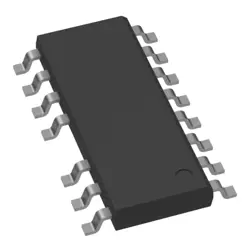
Images are for reference only
ADP7182ACPZN
ADI 200mA Negative Vout LDO
- Manufacturer
- Mfr. Part #ADP7182ACPZN
- Package
- Datasheet
- In Stock17333
100% Original & New
24 Hours ready to ship
365 Days Warranty
RFQ & Get more Discounts
Specifications
| Packaging | Reel |
| Standard Pack Qty | 3000 |
Overview
Description
Key features include low output noise, high power supply rejection ratio (PSRR), and a wide input voltage range of 2.5 V to 20 V. The ADP7182 also includes built-in thermal overload protection, current limiting, and soft-start functionality, enhancing reliability and performance.
The device is packaged in a compact LFCSP (Lead Frame Chip Scale Package), which aids in thermal management and PCB space efficiency. It is ideal for applications such as RF and wireless systems, data converters, and imaging systems, where precision and stability are crucial. Overall, the ADP7182ACPZN is a robust choice for designers seeking high-performance voltage regulation in demanding environments.
Features
1. Output Voltage Range: Adjustable output voltage from 1.2V to 5.0V.
2. Low Dropout Voltage: Typically 200 mV at full load, ensuring efficient operation.
3. High Output Current: Supports up to 1.1 A output current, suitable for a variety of loads.
4. Power Supply Rejection Ratio (PSRR): Excellent PSRR performance, which enhances stability and reduces noise.
5. Thermal Protection: Integrated thermal shutdown to protect against overheating.
6. Short-Circuit Protection: Ensures safe operation under fault conditions.
7. Fast Transient Response: Maintains stability during load transients.
8. Low Quiescent Current: Minimizes power consumption, ideal for battery-operated devices.
9. Small Package: Available in a compact LFCSP package for space-constrained designs.
These features make the ADP7182ACPZN suitable for applications in portable electronics, communication devices, and high-performance analog circuits.
Package
Pinout
1. VIN (Pin 1): Input supply voltage.
2. GND (Pin 2): Ground reference.
3. VOUT (Pin 3): Regulated output voltage.
4. EN (Pin 4): Enable pin for turning the regulator on/off; active high.
5. NC (Pin 5): No connection; typically left floating.
6. VSET (Pin 6): Voltage setting pin used for adjusting the output voltage.
7. COMP (Pin 7): Compensation pin for stability; connects to an external capacitor and resistor.
8. PGND (Pin 8): Power ground; used for high current return paths.
This device provides excellent transient response and power supply rejection, making it suitable for powering sensitive analog circuits.
Manufacturer
Application
Equivalent
Shipping
Shipping MethodsWe
offer global shipping services through DHL, FedEx, TNT, UPS, or any other forwarder of your choice.
Shipping Fee Reference (DHL/FedEx):
DHL: Shipping cost ranges from $25-$45 (0.5kg), with an estimated delivery time of 2-5 business days.
FedEx: Shipping cost ranges from $25-$40 (0.5kg), with an estimated delivery time of 3-7 business days.
UPS: Shipping cost ranges from $25-$45 (0.5kg), with an estimated delivery time of 3-7 business days.
TNT: Shipping cost ranges from $25-$65 (0.5kg), with an estimated delivery time of 3-7 business days.
EMS: Shipping cost ranges from $30-$50 (0.5kg), with an estimated delivery time of 7-15 business days.
Registered Air Mail: Shipping cost is $2-$4 (0.1kg), with an estimated delivery time of 5-20 business days.
Payments
Payment Methods
The Payment term is 100% Prepaid.
Currently, we only accept the below payment methods:
1. PayPal
2. Credit/ Debit Card
3. Wire Transfer
Similar
-
![MX25L3233FM1I-08Q]() MX25L3233FM1I-08Q
MX25L3233FM1I-08Q
Macronix
-
![MX29F400CBTI-70G]() MX29F400CBTI-70G
MX29F400CBTI-70G
Macronix
-
![MX30LF2G28AD-TI]() MX30LF2G28AD-TI
MX30LF2G28AD-TI
Macronix
-
![MX25R6435FBDIL0]() MX25R6435FBDIL0
MX25R6435FBDIL0
Macronix
-
![MX25L25673GMI-08G]() MX25L25673GMI-08G
MX25L25673GMI-08G
Macronix
-
![MX25U25643GZNI00]() MX25U25643GZNI00
MX25U25643GZNI00
Macronix
-
![MX25U6435FM2I-10G]() MX25U6435FM2I-10G
MX25U6435FM2I-10G
Macronix
-
![MX25L12833FZNI-10G]() MX25L12833FZNI-10..
MX25L12833FZNI-10..
Macronix
-
![MX25L25645GXDI-08G]() MX25L25645GXDI-08..
MX25L25645GXDI-08..
Macronix
-
![MX29F040CTI-70G]() MX29F040CTI-70G
MX29F040CTI-70G
Macronix
-
![MX29F800CBTI-70G]() MX29F800CBTI-70G
MX29F800CBTI-70G
Macronix
-
![MX25L25735FMI-10G]() MX25L25735FMI-10G
MX25L25735FMI-10G
Macronix