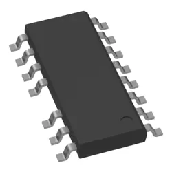
Images are for reference only
AM29F040B-55JF
NOR Flash 4M (512Kx8) 55ns 5v Parallel NOR Flash
- Manufacturer
- Mfr. Part #AM29F040B-55JF
- Package
- Datasheet AM29F040B-55JF DataSheet
- In Stock29312
100% Original & New
24 Hours ready to ship
365 Days Warranty
RFQ & Get more Discounts
Specifications
| Packaging | Tube |
| Standard Pack Qty | 30 |
Overview
Description
The AM29F040B supports standard asynchronous read operations, allowing for quick access times typically around 55 ns. It incorporates a sector-based architecture, enabling partial erasure and programming, which enhances flexibility and efficiency in data management.
Key features include a hardware reset capability, compatibility with a variety of microcontrollers, and a robust design that ensures high endurance and reliability. The device is commonly used in applications such as embedded systems, telecommunications, and consumer electronics, where reliable data storage is critical.
Features
1. Memory Type: It is a CMOS flash memory, providing non-volatile storage.
2. Access Time: The device offers a fast access time of 55 ns, enabling quick read operations.
3. Interface: It supports a byte-wide asynchronous interface, making it compatible with various microcontrollers and processors.
4. Programming: The memory can be programmed in-system or via a programmer, with a typical page programming time of 20 µs.
5. Erase Capability: It supports sector erase, allowing selective erasure of memory blocks for efficient data management.
6. Endurance: The device has a high endurance, typically rated for 10,000 program/erase cycles.
7. Voltage Supply: It operates on a single 5V power supply for read and write operations.
8. Compatibility: It is compatible with JEDEC standards, ensuring ease of integration into existing systems.
These features make the AM29F040B-55JF suitable for various applications, including embedded systems, automotive, and consumer electronics.
Package
Pinout
Pin Count and Functions:
1. Address Pins (A0-A19): 20 pins used to address the memory locations.
2. Data Pins (D0-D7): 8 pins for data input/output.
3. Chip Enable (CE): Activates the device for read/write operations.
4. Output Enable (OE): Controls the output of data from the memory.
5. Write Enable (WE): Enables write operations to the memory.
6. Reset (RESET): Resets the device to a known state.
7. Vcc: Power supply pin.
8. GND: Ground reference.
9. NC (Not Connected): Pins not used internally.
Overall, the AM29F040B-55JF is used primarily for program storage and firmware applications in electronic devices.
Manufacturer
Application
Equivalent
Shipping
Shipping MethodsWe
offer global shipping services through DHL, FedEx, TNT, UPS, or any other forwarder of your choice.
Shipping Fee Reference (DHL/FedEx):
DHL: Shipping cost ranges from $25-$45 (0.5kg), with an estimated delivery time of 2-5 business days.
FedEx: Shipping cost ranges from $25-$40 (0.5kg), with an estimated delivery time of 3-7 business days.
UPS: Shipping cost ranges from $25-$45 (0.5kg), with an estimated delivery time of 3-7 business days.
TNT: Shipping cost ranges from $25-$65 (0.5kg), with an estimated delivery time of 3-7 business days.
EMS: Shipping cost ranges from $30-$50 (0.5kg), with an estimated delivery time of 7-15 business days.
Registered Air Mail: Shipping cost is $2-$4 (0.1kg), with an estimated delivery time of 5-20 business days.
Payments
Payment Methods
The Payment term is 100% Prepaid.
Currently, we only accept the below payment methods:
1. PayPal
2. Credit/ Debit Card
3. Wire Transfer
Similar
-
![MX25R8035FM1IL0]() MX25R8035FM1IL0
MX25R8035FM1IL0
Macronix
-
![MX25V16066M1I02]() MX25V16066M1I02
MX25V16066M1I02
Macronix
-
![MX25L25673GMI-08G]() MX25L25673GMI-08G
MX25L25673GMI-08G
Macronix
-
![MX29GL512FHXFI-11G]() MX29GL512FHXFI-11..
MX29GL512FHXFI-11..
Macronix
-
![MX25R1635FZUIH0]() MX25R1635FZUIH0
MX25R1635FZUIH0
Macronix
-
![MX25L6433FM2I-08G]() MX25L6433FM2I-08G
MX25L6433FM2I-08G
Macronix
-
![MX25L12835FZ2I-10G]() MX25L12835FZ2I-10..
MX25L12835FZ2I-10..
Macronix
-
![MX25L25645GXDI-08G]() MX25L25645GXDI-08..
MX25L25645GXDI-08..
Macronix
-
![MX29F040CTI-70G]() MX29F040CTI-70G
MX29F040CTI-70G
Macronix
-
![MX25L25735FMI-10G]() MX25L25735FMI-10G
MX25L25735FMI-10G
Macronix
-
![MX25U51245GZ4I00]() MX25U51245GZ4I00
MX25U51245GZ4I00
Macronix
-
![MX66U1G45GMI00]() MX66U1G45GMI00
MX66U1G45GMI00
Macronix