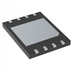
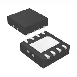
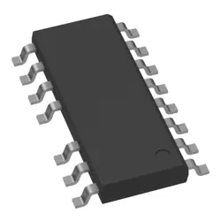
Images are for reference only
AT25SF041B-SSHB-T
IC FLASH 4MBIT SPI/QUAD 8SOIC
- Manufacturer
- Mfr. Part #AT25SF041B-SSHB-T
- Package SOIC-8
- Datasheet
- In Stock4330
100% Original & New
24 Hours ready to ship
365 Days Warranty
RFQ & Get more Discounts
Specifications
| Package | Tape & Reel (TR),Cut Tape (CT) |
| ProductStatus | Active |
| MemoryType | Non-Volatile |
| MemoryFormat | FLASH |
| Technology | FLASH - NOR |
| MemorySize | 4Mb (512K x 8) |
| MemoryInterface | SPI - Quad I/O |
| ClockFrequency | 108 MHz |
| WriteCycleTime-WordPage | 50µs, 2.4ms |
| Voltage-Supply | 2.7V ~ 3.6V |
| OperatingTemperature | -40°C ~ 85°C (TC) |
| MountingType | Surface Mount |
| Package/Case | 8-SOIC (0.154, 3.90mm Width) |
Overview
Description
Key features include fast read speeds of up to 85 MHz, a robust erase capability, and multiple power-saving modes, making it suitable for various applications such as consumer electronics, automotive systems, and industrial controls. The AT25SF041B is available in a compact 8-pin package, facilitating easy integration into space-constrained designs. It supports command-based operations, allowing users to perform a range of functions, including page programming and sector erasing.
Overall, the AT25SF041B-SSHB-T is an ideal choice for applications requiring reliable, high-speed non-volatile memory solutions.
Features
- Density: 4 Mbits (512 Kbytes).
- Supply Voltage: Operates at 2.7V to 3.6V.
- Speed: Fast read speeds of up to 104 MHz, with a dual and quad SPI mode for higher throughput.
- Data Retention: Typically up to 20 years.
- Endurance: 100,000 program/erase cycles.
- Architecture: Supports single, dual, and quad I/O operations.
- Security: Features a 64-bit unique ID and support for a 256-byte security register.
- Package: Available in a compact 8-lead SOIC package.
This memory device is ideal for applications requiring reliable, high-speed data storage, such as consumer electronics, automotive systems, and industrial controls.
Package
Pinout
The functionality of its pins includes:
1. CS (Chip Select): Activates the chip for communication.
2. MOSI (Master Out Slave In): Data input pin for programming and reading.
3. MISO (Master In Slave Out): Data output pin for reading data from the device.
4. SCK (Serial Clock): Clock signal for synchronizing data transmission.
5. VCC: Power supply pin.
6. GND: Ground reference pin.
7. WP (Write Protect): Pin to enable write protection.
8. HOLD: Pin to pause communication.
This component is suitable for various applications requiring non-volatile memory storage.
Manufacturer
Application
Equivalent
1. Micron MT25QL040A
2. Winbond W25Q40BV
3. Cypress S25FL040K
4. Numonyx M25P40
Ensure to check specific pin configurations and voltage requirements for compatibility.
Shipping
Shipping MethodsWe
offer global shipping services through DHL, FedEx, TNT, UPS, or any other forwarder of your choice.
Shipping Fee Reference (DHL/FedEx):
DHL: Shipping cost ranges from $25-$45 (0.5kg), with an estimated delivery time of 2-5 business days.
FedEx: Shipping cost ranges from $25-$40 (0.5kg), with an estimated delivery time of 3-7 business days.
UPS: Shipping cost ranges from $25-$45 (0.5kg), with an estimated delivery time of 3-7 business days.
TNT: Shipping cost ranges from $25-$65 (0.5kg), with an estimated delivery time of 3-7 business days.
EMS: Shipping cost ranges from $30-$50 (0.5kg), with an estimated delivery time of 7-15 business days.
Registered Air Mail: Shipping cost is $2-$4 (0.1kg), with an estimated delivery time of 5-20 business days.
Payments
Payment Methods
The Payment term is 100% Prepaid.
Currently, we only accept the below payment methods:
1. PayPal
2. Credit/ Debit Card
3. Wire Transfer
Similar
-
![MX29F400CBTI-70G]() MX29F400CBTI-70G
Macronix
-
![MX25V2033FM1I]() MX25V2033FM1I
Macronix
-
![MX25V16066M1I02]() MX25V16066M1I02
Macronix
-
![MX25R3235FZNIL0]() MX25R3235FZNIL0
Macronix
-
![MX25R6435FBDIL0]() MX25R6435FBDIL0
Macronix
-
![MX25L2006EM1I-12G]() MX25L2006EM1I-12G
Macronix
-
![MX25L12833FZ2I-10G]() MX25L12833FZ2I-10..
Macronix
-
![MX25L12833FZNI-10G]() MX25L12833FZNI-10..
Macronix
-
![MX25L12835FZ2I-10G]() MX25L12835FZ2I-10..
Macronix
-
![MX29LV160DTTI-70G]() MX29LV160DTTI-70G
Macronix
-
![MX25L25735FMI-10G]() MX25L25735FMI-10G
Macronix
-
![MX30LF4G18AC-TI]() MX30LF4G18AC-TI
Macronix