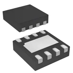
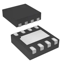
Images are for reference only
BSC0902NSI
MOSFETs N-Ch 30V 100A TDSON-8 OptiMOS
- Manufacturer
- Mfr. Part #BSC0902NSI
- Package
- Datasheet BSC0902NSI DataSheet
- In Stock3323
100% Original & New
24 Hours ready to ship
365 Days Warranty
RFQ & Get more Discounts
Specifications
| Packaging | MouseReel |
| Standard Pack Qty | 5000 |
Overview
Description
Students may engage in laboratory work, field studies, and discussions to enhance their grasp of scientific methods and data interpretation. Assessments usually include quizzes, assignments, and practical experiments, reinforcing theoretical knowledge through hands-on experience. Overall, BSC0902NSI prepares students for more advanced study in biological sciences and related fields, fostering a comprehensive appreciation of the biological world.
Features
1. Frequency Range: Operates effectively in a wide frequency range, typically from 0.1 GHz to 2.5 GHz.
2. Low Noise Figure: Offers a low noise figure, enhancing the overall sensitivity of RF systems.
3. High Gain: Provides significant gain to boost weak signals without distortion, improving signal integrity.
4. Compact Design: Features a small footprint, making it suitable for space-constrained applications.
5. Low Power Consumption: Designed for efficiency, it consumes minimal power while maintaining performance.
6. Temperature Stability: Exhibits stable performance over a wide temperature range, ensuring reliability in various environmental conditions.
7. Integrated Circuit: Combines multiple functionalities into a single chip, simplifying circuit design and reducing component count.
Overall, the BSC0902NSI is ideal for telecommunications, broadcasting, and other RF applications requiring robust performance and reliability.
Package
Pinout
Pin configuration generally includes:
1. Gate 1 (G1) - Controls the first N-channel MOSFET.
2. Drain 1 (D1) - The drain terminal for the first MOSFET.
3. Source 1 (S1) - The source terminal for the first MOSFET.
4. Gate 2 (G2) - Controls the second N-channel MOSFET.
5. Drain 2 (D2) - The drain terminal for the second MOSFET.
6. Source 2 (S2) - The source terminal for the second MOSFET.
7. Unused pin (typically) - May be internally connected or left floating.
8. Common pin (or additional functionality) - Often used for thermal dissipation or grounding.
For specific applications, always refer to the datasheet for detailed operational characteristics and pin functionality.
Manufacturer
Application
Equivalent
Shipping
Shipping MethodsWe
offer global shipping services through DHL, FedEx, TNT, UPS, or any other forwarder of your choice.
Shipping Fee Reference (DHL/FedEx):
DHL: Shipping cost ranges from $25-$45 (0.5kg), with an estimated delivery time of 2-5 business days.
FedEx: Shipping cost ranges from $25-$40 (0.5kg), with an estimated delivery time of 3-7 business days.
UPS: Shipping cost ranges from $25-$45 (0.5kg), with an estimated delivery time of 3-7 business days.
TNT: Shipping cost ranges from $25-$65 (0.5kg), with an estimated delivery time of 3-7 business days.
EMS: Shipping cost ranges from $30-$50 (0.5kg), with an estimated delivery time of 7-15 business days.
Registered Air Mail: Shipping cost is $2-$4 (0.1kg), with an estimated delivery time of 5-20 business days.
Payments
Payment Methods
The Payment term is 100% Prepaid.
Currently, we only accept the below payment methods:
1. PayPal
2. Credit/ Debit Card
3. Wire Transfer
Similar
-
![MX25R8035FM1IL0]() MX25R8035FM1IL0
Macronix
-
![MX25V1635FZNI]() MX25V1635FZNI
Macronix
-
![MX25V1635FZNQ03]() MX25V1635FZNQ03
Macronix
-
![MX29F400CBTI-70G]() MX29F400CBTI-70G
Macronix
-
![MX25V2033FM1I]() MX25V2033FM1I
Macronix
-
![MX25V16066M2I02]() MX25V16066M2I02
Macronix
-
![MX30LF2G28AD-TI]() MX30LF2G28AD-TI
Macronix
-
![MX25R6435FBDIL0]() MX25R6435FBDIL0
Macronix
-
![MX25U51279GXDR00]() MX25U51279GXDR00
Macronix
-
![MX25R1635FZUIH0]() MX25R1635FZUIH0
Macronix
-
![MX25U3232FZBI02]() MX25U3232FZBI02
Macronix
-
![MX25L12833FM2I-10G]() MX25L12833FM2I-10..
Macronix