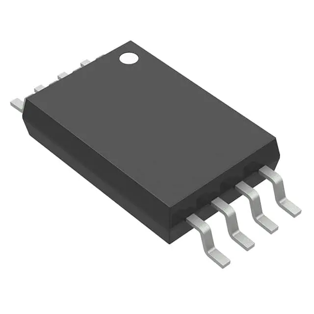
Images are for reference only
CDCLVC1102PWR
IC CLK BUFFER 1:2 250MHZ 8TSSOP
- Manufacturer
- Mfr. Part #CDCLVC1102PWR
- Package TSSOP (PW)-8
- Datasheet
- In Stock2366
100% Original & New
24 Hours ready to ship
365 Days Warranty
RFQ & Get more Discounts
Specifications
| Package | Tape & Reel (TR),Cut Tape (CT) |
| ProductStatus | Active |
| Type | Fanout Buffer (Distribution) |
| NumberofCircuits | 1 |
| Ratio-Input:Output | 1:2 |
| Differential-Input:Output | No/No |
| Input | LVCMOS |
| Output | LVCMOS |
| Frequency-Max | 250 MHz |
| Voltage-Supply | 2.3V ~ 3.6V |
| OperatingTemperature | -40°C ~ 85°C |
| MountingType | Surface Mount |
| Package/Case | 8-TSSOP (0.173, 4.40mm Width) |
Overview
Description
Key features include low power consumption, fast switching speeds, and ease of integration into existing systems. The CDCLVC1102PWR is ideal for applications in portable electronics, IoT devices, and any system requiring stable and reliable voltage level translation. Its compact packaging further enhances its suitability for space-constrained designs. Overall, it provides an efficient solution for ensuring compatibility across different logic levels in modern electronic systems.
Features
1. Input Compatibility: Accepts TTL, CMOS, and LVCMOS input levels.
2. Output Configuration: Offers two outputs with low skew, ensuring high signal integrity.
3. Low Power Consumption: Designed for energy efficiency, making it suitable for battery-operated devices.
4. Voltage Range: Operates within a voltage range of 1.8V to 3.6V, catering to various system requirements.
5. High Speed: Supports high-frequency clock signals, ideal for fast data transfer applications.
6. Packaging: Available in a small footprint, making it suitable for space-constrained designs.
7. Temperature Range: Operates reliably across an extended temperature range, ensuring stable performance in diverse environments.
Overall, the CDCLVC1102PWR is a versatile and efficient solution for clock distribution needs in modern electronic systems.
Package
Pinout
The primary functions include:
- Buffers two differential input clocks, providing increased signal integrity and reduced skew.
- Outputs can drive multiple loads with low jitter.
- Supports both single-ended and differential signaling.
Key pins include:
- Inputs (A, B): Receive the differential clock signals.
- Outputs (Y, Z): Deliver buffered clock signals, both differential and single-ended options.
- OE (Output Enable): Controls the enabling/disabling of the output buffers.
- VDD/VSS: Power supply and ground pins.
- GND: Ground connection.
This device is commonly used in high-speed clock distribution applications in systems requiring precise timing, such as telecommunications and data communication.
Manufacturer
Application
Equivalent
Shipping
Shipping MethodsWe
offer global shipping services through DHL, FedEx, TNT, UPS, or any other forwarder of your choice.
Shipping Fee Reference (DHL/FedEx):
DHL: Shipping cost ranges from $25-$45 (0.5kg), with an estimated delivery time of 2-5 business days.
FedEx: Shipping cost ranges from $25-$40 (0.5kg), with an estimated delivery time of 3-7 business days.
UPS: Shipping cost ranges from $25-$45 (0.5kg), with an estimated delivery time of 3-7 business days.
TNT: Shipping cost ranges from $25-$65 (0.5kg), with an estimated delivery time of 3-7 business days.
EMS: Shipping cost ranges from $30-$50 (0.5kg), with an estimated delivery time of 7-15 business days.
Registered Air Mail: Shipping cost is $2-$4 (0.1kg), with an estimated delivery time of 5-20 business days.
Payments
Payment Methods
The Payment term is 100% Prepaid.
Currently, we only accept the below payment methods:
1. PayPal
2. Credit/ Debit Card
3. Wire Transfer
Similar
-
![MX25R8035FM1IL0]() MX25R8035FM1IL0
Macronix
-
![MX25L3233FM1I-08Q]() MX25L3233FM1I-08Q
Macronix
-
![MX25V2033FM1I]() MX25V2033FM1I
Macronix
-
![MX25V16066M1I02]() MX25V16066M1I02
Macronix
-
![MX25R3235FZNIL0]() MX25R3235FZNIL0
Macronix
-
![MX25R6435FBDIL0]() MX25R6435FBDIL0
Macronix
-
![MX25L25673GMI-08G]() MX25L25673GMI-08G
Macronix
-
![MX25U25643GZNI00]() MX25U25643GZNI00
Macronix
-
![MX25L2006EM1I-12G]() MX25L2006EM1I-12G
Macronix
-
![MX25L12833FM2I-10G]() MX25L12833FM2I-10..
Macronix
-
![MX25L25645GXDI-08G]() MX25L25645GXDI-08..
Macronix
-
![MX29F800CBTI-70G]() MX29F800CBTI-70G
Macronix