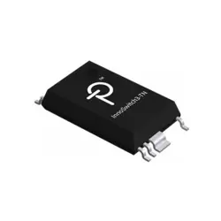
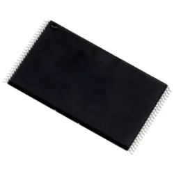
Images are for reference only
CDCLVC1108PWR
IC CLK BUFFER 1:8 250MHZ 16TSSOP
- Manufacturer
- Mfr. Part #CDCLVC1108PWR
- Package TSSOP-16
- Datasheet
- In Stock2172
100% Original & New
24 Hours ready to ship
365 Days Warranty
RFQ & Get more Discounts
Specifications
| Package | Tape & Reel (TR),Cut Tape (CT) |
| ProductStatus | Active |
| Type | Fanout Buffer (Distribution) |
| NumberofCircuits | 1 |
| Ratio-Input:Output | 1:8 |
| Differential-Input:Output | No/No |
| Input | LVCMOS |
| Output | LVCMOS |
| Frequency-Max | 250 MHz |
| Voltage-Supply | 2.3V ~ 3.6V |
| OperatingTemperature | -40°C ~ 85°C |
| MountingType | Surface Mount |
| Package/Case | 16-TSSOP (0.173, 4.40mm Width) |
Overview
Description
Key features include a wide supply voltage range, low propagation delay, and the ability to operate with various input signal levels. The CDCLVC1108PWR supports both single-ended and differential input modes, making it versatile for different applications. Its low skew characteristics ensure that all outputs switch in unison, critical for high-speed digital circuits.
Additionally, the device is packaged in a compact form, suitable for space-constrained designs. It is ideal for use in data communication, networking, and other high-speed digital applications where reliable clock distribution is essential. Overall, the CDCLVC1108PWR combines efficiency and performance, making it a valuable component in modern electronic systems.
Features
1. Low Voltage Operation: Supports a supply voltage range of 1.65V to 3.6V, ideal for modern low-power systems.
2. Output Capability: Drives up to eight outputs, making it suitable for multi-channel applications.
3. Low Jitter: Offers low clock jitter, ensuring high signal integrity for demanding applications.
4. Fanout: Provides high fanout, allowing one clock input to drive multiple loads without signal degradation.
5. Single-Ended Inputs: Compatible with single-ended clock inputs, simplifying integration with various circuitry.
6. Power Management: Features power-down modes to conserve energy when not in use.
7. Temperature Range: Operates over a wide temperature range, ensuring reliability in diverse environments.
Its versatility makes it suitable for telecom, networking, and consumer electronics applications, ensuring efficient clock management and distribution.
Package
Pinout
- Input/Output: The device has a single clock input (CLK) and eight clock outputs (Q0 to Q7).
- Control Pins: It includes control pins such as EN (enable), which allows for enabling or disabling the outputs, and a few configuration pins for output settings.
- Power Supply: It operates typically at 3.3V and has power supply pins (VCC and GND).
This device is designed to distribute clock signals with low skew and high integrity, making it suitable for various high-speed applications.
Manufacturer
Application
Equivalent
Shipping
Shipping MethodsWe
offer global shipping services through DHL, FedEx, TNT, UPS, or any other forwarder of your choice.
Shipping Fee Reference (DHL/FedEx):
DHL: Shipping cost ranges from $25-$45 (0.5kg), with an estimated delivery time of 2-5 business days.
FedEx: Shipping cost ranges from $25-$40 (0.5kg), with an estimated delivery time of 3-7 business days.
UPS: Shipping cost ranges from $25-$45 (0.5kg), with an estimated delivery time of 3-7 business days.
TNT: Shipping cost ranges from $25-$65 (0.5kg), with an estimated delivery time of 3-7 business days.
EMS: Shipping cost ranges from $30-$50 (0.5kg), with an estimated delivery time of 7-15 business days.
Registered Air Mail: Shipping cost is $2-$4 (0.1kg), with an estimated delivery time of 5-20 business days.
Payments
Payment Methods
The Payment term is 100% Prepaid.
Currently, we only accept the below payment methods:
1. PayPal
2. Credit/ Debit Card
3. Wire Transfer
Similar
-
![MX25V1635FZNQ03]() MX25V1635FZNQ03
MX25V1635FZNQ03
Macronix
-
![MX29F400CBTI-70G]() MX29F400CBTI-70G
MX29F400CBTI-70G
Macronix
-
![MX25V16066M2I02]() MX25V16066M2I02
MX25V16066M2I02
Macronix
-
![MX25L25673GMI-10G]() MX25L25673GMI-10G
MX25L25673GMI-10G
Macronix
-
![MX25U25643GZNI00]() MX25U25643GZNI00
MX25U25643GZNI00
Macronix
-
![MX25L6433FM2I-08G]() MX25L6433FM2I-08G
MX25L6433FM2I-08G
Macronix
-
![MX25L12833FM2I-10G]() MX25L12833FM2I-10..
MX25L12833FM2I-10..
Macronix
-
![MX25L12835FZ2I-10G]() MX25L12835FZ2I-10..
MX25L12835FZ2I-10..
Macronix
-
![MX25L25645GXDI-08G]() MX25L25645GXDI-08..
MX25L25645GXDI-08..
Macronix
-
![MX25L1006EMI-10G]() MX25L1006EMI-10G
MX25L1006EMI-10G
Macronix
-
![MX66U1G45GMI00]() MX66U1G45GMI00
MX66U1G45GMI00
Macronix
-
![MX30LF4G28AD-TI]() MX30LF4G28AD-TI
MX30LF4G28AD-TI
Macronix