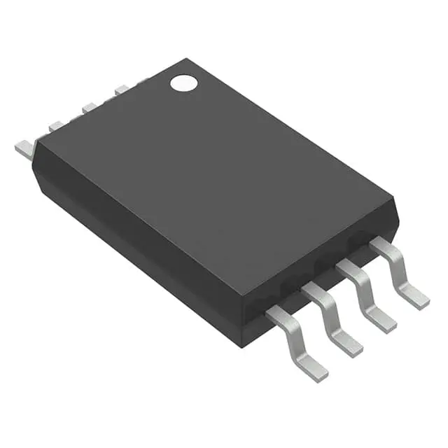
Images are for reference only
CDCVF2505PWR
IC 3.3V PLL CLOCK DRVR 8-TSSOP
- Manufacturer
- Mfr. Part #CDCVF2505PWR
- Package TSSOP8
- Datasheet
- In Stock4114
100% Original & New
24 Hours ready to ship
365 Days Warranty
RFQ & Get more Discounts
Specifications
| Package | Tape & Reel (TR),Cut Tape (CT) |
| ProductStatus | Active |
| Type | PLL Clock Driver |
| PLL | Yes with Bypass |
| Input | LVTTL |
| Output | LVTTL |
| NumberofCircuits | 1 |
| Ratio-Input:Output | 1:5 |
| Differential-Input:Output | No/No |
| Frequency-Max | 200MHz |
| Divider/Multiplier | No/No |
| Voltage-Supply | 3V ~ 3.6V |
| OperatingTemperature | -40°C ~ 85°C |
| MountingType | Surface Mount |
| Package/Case | 8-TSSOP (0.173, 4.40mm Width) |
Overview
Description
Key features include:
- Wide operating voltage range (1.1V to 5.5V)
- Bidirectional data flow capabilities
- Low input and output capacitance
- High-speed operation, supporting data rates up to 100 Mbps
- Small package size, facilitating integration into compact designs
Engineered for reliability, the CDCVF2505PWR ensures signal integrity across different voltage domains, making it ideal for modern digital systems where interoperability is crucial.
Features
1. Multiple Output Frequencies: It can produce multiple output clock frequencies derived from a single input clock.
2. Low Phase Jitter: Provides excellent timing stability, which is crucial for high-speed applications.
3. Wide Supply Voltage Range: Operates typically between 2.3V and 3.6V, accommodating various system requirements.
4. Power Efficiency: Consumes low power, making it suitable for battery-operated devices.
5. Flexible Output Format: Outputs can be configured for different standards, such as CMOS and LVTTL.
6. Single Output Enable Control: Facilitates easy management of output signals.
7. Temperature Range: Rated for operation across a wide temperature range, enhancing reliability in diverse environments.
These features make the CDCVF2505PWR suitable for applications like telecommunications, data communications, and consumer electronics.
Package
Pinout
The primary functions of the CDCVF2505PWR include:
- Signal Translation: It translates logic levels between different voltage thresholds, allowing communication between devices operating at varying supply voltages.
- Clock Distribution: It distributes clock signals to multiple outputs, ensuring synchronization across connected devices.
- Buffering: It provides buffering to improve signal integrity and drive capability, minimizing signal degradation over distance.
The device is particularly useful in applications involving mixed-voltage systems, where it helps maintain signal integrity while facilitating interoperability among components with different voltage requirements.
Manufacturer
Application
Equivalent
1. SN74CBT3245PWR
2. SN74LVDS32A
3. SN74LS125A
4. SN74LVTH16244
Ensure compatibility in terms of voltage levels, package type, and functionality before substitution. Always consult datasheets for specific requirements.
Shipping
Shipping MethodsWe
offer global shipping services through DHL, FedEx, TNT, UPS, or any other forwarder of your choice.
Shipping Fee Reference (DHL/FedEx):
DHL: Shipping cost ranges from $25-$45 (0.5kg), with an estimated delivery time of 2-5 business days.
FedEx: Shipping cost ranges from $25-$40 (0.5kg), with an estimated delivery time of 3-7 business days.
UPS: Shipping cost ranges from $25-$45 (0.5kg), with an estimated delivery time of 3-7 business days.
TNT: Shipping cost ranges from $25-$65 (0.5kg), with an estimated delivery time of 3-7 business days.
EMS: Shipping cost ranges from $30-$50 (0.5kg), with an estimated delivery time of 7-15 business days.
Registered Air Mail: Shipping cost is $2-$4 (0.1kg), with an estimated delivery time of 5-20 business days.
Payments
Payment Methods
The Payment term is 100% Prepaid.
Currently, we only accept the below payment methods:
1. PayPal
2. Credit/ Debit Card
3. Wire Transfer
Similar
-
![MX25R8035FM1IL0]() MX25R8035FM1IL0
MX25R8035FM1IL0
Macronix
-
![MX25L3233FM1I-08Q]() MX25L3233FM1I-08Q
MX25L3233FM1I-08Q
Macronix
-
![MX25V5126FM1I]() MX25V5126FM1I
MX25V5126FM1I
Macronix
-
![MX25V16066M2I02]() MX25V16066M2I02
MX25V16066M2I02
Macronix
-
![MX25R6435FBDIL0]() MX25R6435FBDIL0
MX25R6435FBDIL0
Macronix
-
![MX25R1635FZUIH0]() MX25R1635FZUIH0
MX25R1635FZUIH0
Macronix
-
![MX25V1635FM2I]() MX25V1635FM2I
MX25V1635FM2I
Macronix
-
![MX25L6433FM2I-08G]() MX25L6433FM2I-08G
MX25L6433FM2I-08G
Macronix
-
![MX25L12833FM2I-10G]() MX25L12833FM2I-10..
MX25L12833FM2I-10..
Macronix
-
![MX25U25645GXDI00]() MX25U25645GXDI00
MX25U25645GXDI00
Macronix
-
![MX29LV160DTTI-70G]() MX29LV160DTTI-70G
MX29LV160DTTI-70G
Macronix
-
![MX29F040CQI-70G]() MX29F040CQI-70G
MX29F040CQI-70G
Macronix