
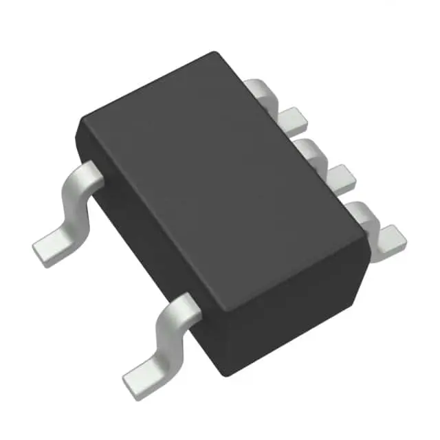
Images are for reference only
CLVC1G125IDCKREP
IC BUF NON-INVERT 5.5V SC70-5
- Manufacturer
- Mfr. Part #CLVC1G125IDCKREP
- Package SOT-SC70 (DCK)-5
- Datasheet
- In Stock7999
100% Original & New
24 Hours ready to ship
365 Days Warranty
RFQ & Get more Discounts
Specifications
| Package | Tape & Reel (TR),Cut Tape (CT),Bulk |
| Series | 74LVC |
| ProductStatus | Active |
| LogicType | Buffer, Non-Inverting |
| NumberofElements | 1 |
| NumberofBitsperElement | 1 |
| OutputType | 3-State |
| Current-OutputHighLow | 32mA, 32mA |
| Voltage-Supply | 1.65V ~ 5.5V |
| OperatingTemperature | -40°C ~ 85°C (TA) |
| MountingType | Surface Mount |
| Package/Case | 5-TSSOP, SC-70-5, SOT-353 |
Overview
Description
The packaging is typically in a SC70-5, which allows for space-saving designs in compact electronic applications. The CLVC1G125IDCKREP is widely used in consumer electronics, automotive systems, and telecommunications. Its robust performance and versatility make it a popular choice among engineers designing high-speed digital circuits.
Features
1. Voltage Range: Operates from a supply voltage of 1.65V to 5.5V, making it suitable for various logic levels.
2. High Speed: Capable of switching speeds up to 10 ns at Vcc = 5V, ensuring fast data transmission.
3. Low Power Consumption: Designed for minimal static and dynamic power dissipation, enhancing overall efficiency in battery-operated devices.
4. Schmitt-Trigger Input: Provides improved noise immunity and faster transitions for signals.
5. Fan-out Capability: Can drive multiple loads, supporting high fan-out applications.
6. Compact Package: Available in a small SC70-5 package for space-constrained designs.
7. Wide Operating Temp Range: Suitable for industrial applications with an operating temperature range from -40°C to 125°C.
Overall, the CLVC1G125IDCKREP is ideal for buffer applications in portable and consumer electronics.
Package
Pinout
Pin Count: 5 pins
Pin Functions:
1. A (Input): The data input pin where the signal is received.
2. Y (Output): The output pin that drives the signal based on the input state.
3. GND (Ground): The ground reference for the device.
4. VCC (Power Supply): The positive power supply pin, typically between 1.65V and 5.5V.
5. OE (Output Enable): A control pin that enables or disables the output; when high, the output is active.
This device is characterized by low power consumption and high-speed operation, making it suitable for various digital applications. It operates under a voltage range of 1.65V to 5.5V, ensuring compatibility with various logic levels.
Manufacturer
Application
Equivalent
1. SN74LVC1G125 - Texas Instruments
2. 74LVC1G125 - NXP Semiconductors
3. MC74LCX1G125 - ON Semiconductor
Ensure to check specifications like voltage levels and pin configurations for compatibility.
Shipping
Shipping MethodsWe
offer global shipping services through DHL, FedEx, TNT, UPS, or any other forwarder of your choice.
Shipping Fee Reference (DHL/FedEx):
DHL: Shipping cost ranges from $25-$45 (0.5kg), with an estimated delivery time of 2-5 business days.
FedEx: Shipping cost ranges from $25-$40 (0.5kg), with an estimated delivery time of 3-7 business days.
UPS: Shipping cost ranges from $25-$45 (0.5kg), with an estimated delivery time of 3-7 business days.
TNT: Shipping cost ranges from $25-$65 (0.5kg), with an estimated delivery time of 3-7 business days.
EMS: Shipping cost ranges from $30-$50 (0.5kg), with an estimated delivery time of 7-15 business days.
Registered Air Mail: Shipping cost is $2-$4 (0.1kg), with an estimated delivery time of 5-20 business days.
Payments
Payment Methods
The Payment term is 100% Prepaid.
Currently, we only accept the below payment methods:
1. PayPal
2. Credit/ Debit Card
3. Wire Transfer
Similar
-
![MX25R8035FM1IL0]() MX25R8035FM1IL0
MX25R8035FM1IL0
Macronix
-
![MX25V1635FZNI]() MX25V1635FZNI
MX25V1635FZNI
Macronix
-
![MX29F400CBTI-70G]() MX29F400CBTI-70G
MX29F400CBTI-70G
Macronix
-
![MX25V4035FZUI]() MX25V4035FZUI
MX25V4035FZUI
Macronix
-
![MX25V2033FM1I]() MX25V2033FM1I
MX25V2033FM1I
Macronix
-
![MX25V16066M1I02]() MX25V16066M1I02
MX25V16066M1I02
Macronix
-
![MX25R3235FZNIL0]() MX25R3235FZNIL0
MX25R3235FZNIL0
Macronix
-
![MX25L8035EM2I-10G]() MX25L8035EM2I-10G
MX25L8035EM2I-10G
Macronix
-
![MX25R6435FBDIL0]() MX25R6435FBDIL0
MX25R6435FBDIL0
Macronix
-
![MX29GL512FHXFI-11G]() MX29GL512FHXFI-11..
MX29GL512FHXFI-11..
Macronix
-
![MX25U51279GXDR00]() MX25U51279GXDR00
MX25U51279GXDR00
Macronix
-
![MX25U25643GZNI00]() MX25U25643GZNI00
MX25U25643GZNI00
Macronix




