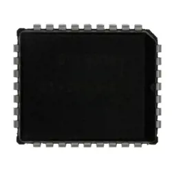
Images are for reference only
CY7B933-JXI
IC RECEIVER 28PLCC
- Manufacturer
- Mfr. Part #CY7B933-JXI
- Package PLCC-28
- Datasheet CY7B933-JXI DataSheet
- In Stock3876
100% Original & New
24 Hours ready to ship
365 Days Warranty
RFQ & Get more Discounts
Specifications
| Package | Tube,Tube |
| Series | HOTlink™ |
| ProductStatus | Active |
| Type | Receiver |
| Protocol | Fibre Channel |
| Voltage-Supply | 4.5V ~ 5.5V |
| OperatingTemperature | 0°C ~ 70°C |
| MountingType | Surface Mount |
| Package/Case | 28-LCC (J-Lead) |
Overview
Description
Key features include low power consumption, ease of integration, and wide operating voltage ranges. It has programmable features such as programmable flags for empty and full conditions, ensuring reliable operation in data flow management. The CY7B933-JXI is commonly used in systems requiring temporary data storage, such as telecommunications, video processing, and industrial control applications. With a fast access time and minimal latency, it is ideal for real-time applications where speed is critical. Overall, the CY7B933-JXI combines functionality with robust performance, making it a suitable choice for designers seeking efficient data handling solutions.
Features
- Memory Configuration: It is typically organized as 256K x 16 bits.
- Access Speed: Offers fast access times, typically around 10 ns, suitable for high-performance applications.
- Operating Voltage: Supports a wide operating voltage range, generally from 2.7V to 3.6V.
- Power Consumption: Low power consumption in active and standby modes, making it energy-efficient.
- Interface: Compatible with standard SRAM interface protocols, facilitating easy integration into various systems.
- Packaging: Available in different package options, including TQFP and BGA, for flexibility in design.
- Applications: Commonly used in telecommunications, networking, consumer electronics, and industrial applications due to its reliability and speed.
These features make the CY7B933-JXI a suitable choice for applications requiring fast, reliable memory solutions.
Package
Pinout
1. Data I/O (D0-D7): 8-bit data bus for read and write operations.
2. Address Inputs (A0-A14): 15 address lines to access the memory locations.
3. Chip Enable (CE): Activates the chip for read/write operations.
4. Output Enable (OE): Controls the output buffers to enable data output.
5. Write Enable (WE): Determines when data is written to the SRAM.
6. Clock (CLK): Synchronizes the read and write operations.
7. Byte Enable (BE): Allows for byte-wide access in write operations.
Always refer to the specific datasheet for detailed pin descriptions and electrical characteristics.
Manufacturer
Application
Equivalent
Shipping
Shipping MethodsWe
offer global shipping services through DHL, FedEx, TNT, UPS, or any other forwarder of your choice.
Shipping Fee Reference (DHL/FedEx):
DHL: Shipping cost ranges from $25-$45 (0.5kg), with an estimated delivery time of 2-5 business days.
FedEx: Shipping cost ranges from $25-$40 (0.5kg), with an estimated delivery time of 3-7 business days.
UPS: Shipping cost ranges from $25-$45 (0.5kg), with an estimated delivery time of 3-7 business days.
TNT: Shipping cost ranges from $25-$65 (0.5kg), with an estimated delivery time of 3-7 business days.
EMS: Shipping cost ranges from $30-$50 (0.5kg), with an estimated delivery time of 7-15 business days.
Registered Air Mail: Shipping cost is $2-$4 (0.1kg), with an estimated delivery time of 5-20 business days.
Payments
Payment Methods
The Payment term is 100% Prepaid.
Currently, we only accept the below payment methods:
1. PayPal
2. Credit/ Debit Card
3. Wire Transfer
Similar
-
![MX25L3233FM1I-08Q]() MX25L3233FM1I-08Q
Macronix
-
![MX25V1635FZNI]() MX25V1635FZNI
Macronix
-
![MX25V5126FM1I]() MX25V5126FM1I
Macronix
-
![MX25V2033FM1I]() MX25V2033FM1I
Macronix
-
![MX25R3235FZNIL0]() MX25R3235FZNIL0
Macronix
-
![MX25V16066M2I02]() MX25V16066M2I02
Macronix
-
![MX25U51279GXDR00]() MX25U51279GXDR00
Macronix
-
![MX25V1635FM2I]() MX25V1635FM2I
Macronix
-
![MX25U25645GXDI00]() MX25U25645GXDI00
Macronix
-
![MX29F040CQI-70G]() MX29F040CQI-70G
Macronix
-
![MX29F800CBTI-70G]() MX29F800CBTI-70G
Macronix
-
![MX29LV640ETTI-70G]() MX29LV640ETTI-70G
Macronix