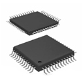
Images are for reference only
EP2C15AF484C8N
IC FPGA 315 I/O 484FBGA
- Manufacturer
- Mfr. Part #EP2C15AF484C8N
- Package
- Datasheet EP2C15AF484C8N DataSheet
- In Stock4366
100% Original & New
24 Hours ready to ship
365 Days Warranty
RFQ & Get more Discounts
Specifications
| Series | Cyclone® II |
| Part Status | Active |
| DigiKey Programmable | Not Verified |
| Total RAM Bits | 239616 |
| Number of I/O | 315 |
| Voltage - Supply | 1.15V ~ 1.25V |
| Mounting Type | Surface Mount |
| Operating Temperature | 0°C ~ 85°C (TJ) |
| Package / Case | 484-BGA |
| Supplier Device Package | 484-FBGA (23x23) |
| Base Product Number | EP2C15 |
| Number of Logic Elements/Cells | 14448 |
| Number of LABs/CLBs | 903 |
Overview
Description
The FPGA is designed for low power consumption and offers a combination of programmable logic resources, embedded memory, and digital signal processing (DSP) capabilities. It supports a range of development tools, including Quartus Prime, making it accessible for developers working on applications like communications, automotive systems, and consumer electronics. Overall, the EP2C15AF484C8N is ideal for projects requiring flexibility, performance, and efficient resource utilization.
Features
1. Logic Elements: It contains 15,000 logic elements, which are configurable for various logic functions.
2. Memory: The device has embedded memory blocks, providing up to 576 Kbits of RAM.
3. I/O Pins: It features 484 pins with up to 32 I/O pins capable of supporting various voltage levels.
4. Performance: The FPGA operates at speeds up to 160 MHz, suitable for high-performance applications.
5. Power Consumption: It is designed for low power consumption, making it ideal for portable and battery-operated devices.
6. Development Tools: Compatible with Intel’s Quartus Prime software, providing robust design tools for development.
7. Programmability: Offers reprogrammability, allowing for design updates and changes as needed.
The EP2C15AF484C8N is suitable for various applications, including digital signal processing, embedded systems, and communication devices.
Package
Pinout
The primary functions of the EP2C15AF484C8N include:
- Configurable logic blocks (CLBs) for implementing logic functions.
- Flexible I/O pins for interfacing with other devices and systems.
- Built-in memory blocks (like RAM) for data storage.
- Support for high-speed serial interfaces.
- Programmable interconnect for routing signals between logic elements.
This FPGA is suitable for cost-sensitive applications that require moderate logic resources and performance.
Manufacturer
Application
Equivalent
Shipping
Shipping MethodsWe
offer global shipping services through DHL, FedEx, TNT, UPS, or any other forwarder of your choice.
Shipping Fee Reference (DHL/FedEx):
DHL: Shipping cost ranges from $25-$45 (0.5kg), with an estimated delivery time of 2-5 business days.
FedEx: Shipping cost ranges from $25-$40 (0.5kg), with an estimated delivery time of 3-7 business days.
UPS: Shipping cost ranges from $25-$45 (0.5kg), with an estimated delivery time of 3-7 business days.
TNT: Shipping cost ranges from $25-$65 (0.5kg), with an estimated delivery time of 3-7 business days.
EMS: Shipping cost ranges from $30-$50 (0.5kg), with an estimated delivery time of 7-15 business days.
Registered Air Mail: Shipping cost is $2-$4 (0.1kg), with an estimated delivery time of 5-20 business days.
Payments
Payment Methods
The Payment term is 100% Prepaid.
Currently, we only accept the below payment methods:
1. PayPal
2. Credit/ Debit Card
3. Wire Transfer
Similar
-
![MX25R8035FM1IL0]() MX25R8035FM1IL0
Macronix
-
![MX25V1635FZNI]() MX25V1635FZNI
Macronix
-
![MX29F400CBTI-70G]() MX29F400CBTI-70G
Macronix
-
![MX25V5126FM1I]() MX25V5126FM1I
Macronix
-
![MX30LF2G28AD-TI]() MX30LF2G28AD-TI
Macronix
-
![MX25L25673GMI-08G]() MX25L25673GMI-08G
Macronix
-
![MX25L25673GMI-10G]() MX25L25673GMI-10G
Macronix
-
![MX25L2006EM1I-12G]() MX25L2006EM1I-12G
Macronix
-
![MX25R1635FZUIH0]() MX25R1635FZUIH0
Macronix
-
![MX25V1635FM2I]() MX25V1635FM2I
Macronix
-
![MX25L12833FM2I-10G]() MX25L12833FM2I-10..
Macronix
-
![MX25L12833FZNI-10G]() MX25L12833FZNI-10..
Macronix