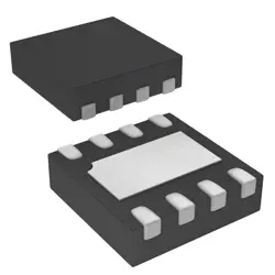
Images are for reference only
EP2S30F484I4N
IC FPGA 342 I/O 484FBGA
- Manufacturer
- Mfr. Part #EP2S30F484I4N
- Package FBGA-484
- Datasheet
- In Stock3366
100% Original & New
24 Hours ready to ship
365 Days Warranty
RFQ & Get more Discounts
Specifications
| Package | Tray |
| Series | Stratix® II |
| ProductStatus | Obsolete |
| NumberofLABs/CLBs | 1694 |
| NumberofLogicElements/Cells | 33880 |
| TotalRAMBits | 1369728 |
| NumberofI/O | 342 |
| Voltage-Supply | 1.15V ~ 1.25V |
| MountingType | Surface Mount |
| OperatingTemperature | -40°C ~ 100°C (TJ) |
| Package/Case | 484-BBGA |
Overview
Description
Key features include:
- Logic Density: Offers a significant number of logic elements and supports a range of I/O configurations.
- Memory: Integrated memory blocks facilitate efficient data handling and storage.
- High-Speed Performance: Capable of handling high-speed data rates, suitable for demanding tasks.
- Flexibility: As an FPGA, it allows users to configure hardware based on their specific application requirements.
- Development Tools: Supported by Intel’s Quartus Prime software for design, simulation, and deployment.
The EP2S30F484I4N is widely used in industries such as telecommunications, automotive, and aerospace, where custom hardware solutions are essential for optimized performance.
Features
1. Logic Elements: It has around 30,000 logic elements, enabling complex designs.
2. Memory: Supports up to 1.5 Mbits of on-chip memory, facilitating efficient data storage.
3. I/O Pins: The package includes 484 pins with various I/O standards, supporting high-speed data transfer.
4. DSP Blocks: Integrated DSP blocks enhance processing capabilities for digital signal applications.
5. Configuration: Offers flexible configuration options, including JTAG and passive serial modes.
6. Power Consumption: Designed for low power consumption, making it suitable for energy-sensitive applications.
7. Performance: Features high-speed transceivers, supporting multiple protocols for versatile connectivity.
This FPGA is ideal for telecommunications, automotive, and industrial applications where performance and flexibility are crucial.
Package
Pinout
The functions of the pins include:
- Configurable I/O pins for general-purpose digital input/output.
- Power pins for supplying core and I/O voltages.
- Ground pins.
- Dedicated configuration pins for programming the FPGA.
- Clock input pins for providing clock signals to the device.
- Special function pins for features like JTAG for in-system programming and debugging.
This FPGA is designed for high-performance applications, offering a balance between logic capacity and I/O capabilities, making it suitable for various digital signal processing, networking, and data processing tasks.
Manufacturer
Application
Equivalent
Shipping
Shipping MethodsWe
offer global shipping services through DHL, FedEx, TNT, UPS, or any other forwarder of your choice.
Shipping Fee Reference (DHL/FedEx):
DHL: Shipping cost ranges from $25-$45 (0.5kg), with an estimated delivery time of 2-5 business days.
FedEx: Shipping cost ranges from $25-$40 (0.5kg), with an estimated delivery time of 3-7 business days.
UPS: Shipping cost ranges from $25-$45 (0.5kg), with an estimated delivery time of 3-7 business days.
TNT: Shipping cost ranges from $25-$65 (0.5kg), with an estimated delivery time of 3-7 business days.
EMS: Shipping cost ranges from $30-$50 (0.5kg), with an estimated delivery time of 7-15 business days.
Registered Air Mail: Shipping cost is $2-$4 (0.1kg), with an estimated delivery time of 5-20 business days.
Payments
Payment Methods
The Payment term is 100% Prepaid.
Currently, we only accept the below payment methods:
1. PayPal
2. Credit/ Debit Card
3. Wire Transfer
Similar
-
![MX25L3233FM1I-08Q]() MX25L3233FM1I-08Q
MX25L3233FM1I-08Q
Macronix
-
![MX25V5126FM1I]() MX25V5126FM1I
MX25V5126FM1I
Macronix
-
![MX25V4035FZUI]() MX25V4035FZUI
MX25V4035FZUI
Macronix
-
![MX25V16066M2I02]() MX25V16066M2I02
MX25V16066M2I02
Macronix
-
![MX30LF2G28AD-TI]() MX30LF2G28AD-TI
MX30LF2G28AD-TI
Macronix
-
![MX25L8035EM2I-10G]() MX25L8035EM2I-10G
MX25L8035EM2I-10G
Macronix
-
![MX25R6435FBDIL0]() MX25R6435FBDIL0
MX25R6435FBDIL0
Macronix
-
![MX25U51279GXDR00]() MX25U51279GXDR00
MX25U51279GXDR00
Macronix
-
![MX25U25643GZNI00]() MX25U25643GZNI00
MX25U25643GZNI00
Macronix
-
![MX25V1635FM2I]() MX25V1635FM2I
MX25V1635FM2I
Macronix
-
![MX25U3232FZBI02]() MX25U3232FZBI02
MX25U3232FZBI02
Macronix
-
![MX25L12833FZ2I-10G]() MX25L12833FZ2I-10..
MX25L12833FZ2I-10..
Macronix