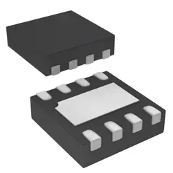
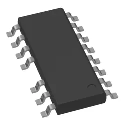
Images are for reference only
FDG6332C
MOSFET N/P-CH 20V SC70-6
- Manufacturer
- Mfr. Part #FDG6332C
- Package TSSOP-6
- Datasheet
- In Stock6300
100% Original & New
24 Hours ready to ship
365 Days Warranty
RFQ & Get more Discounts
Specifications
| Package | Tape & Reel (TR),Cut Tape (CT) |
| Series | PowerTrench® |
| ProductStatus | Active |
| FETType | N and P-Channel |
| FETFeature | Logic Level Gate |
| DraintoSourceVoltage(Vdss) | 20V |
| Current-ContinuousDrain(Id)@25°C | 700mA, 600mA |
| RdsOn(Max)@IdVgs | 300mOhm @ 700mA, 4.5V |
| Vgs(th)(Max)@Id | 1.5V @ 250µA |
| GateCharge(Qg)(Max)@Vgs | 1.5nC @ 4.5V |
| InputCapacitance(Ciss)(Max)@Vds | 113pF @ 10V |
| Power-Max | 300mW |
| OperatingTemperature | -55°C ~ 150°C (TJ) |
| MountingType | Surface Mount |
| Package/Case | 6-TSSOP, SC-88, SOT-363 |
Overview
Description
Students are likely to engage in case studies, group projects, and discussions to deepen their understanding of complex issues and develop problem-solving skills. Emphasis may be placed on real-world applications and current trends, preparing participants for advanced roles in their respective industries.
Overall, FDG6332C aims to equip students with the knowledge and skills necessary for effective analysis and decision-making in a professional context.
Features
1. Wide Input Voltage Range: Supports inputs from 4.5V to 20V, suitable for various power sources.
2. Adjustable Output Voltage: Configurable output voltage settings down to 0.8V, allowing for flexibility in applications.
3. High Efficiency: Offers up to 95% efficiency, minimizing power loss and heat generation during operation.
4. Output Current Capability: Can deliver up to 3A per channel, accommodating high-power devices.
5. Integrated Compensation: Built-in compensation simplifies circuit design and ensures stable operation.
6. Thermal Protection: Features over-temperature protection to prevent damage under excessive heat conditions.
7. Short-Circuit Protection: Protects the device from damage due to unexpected short circuits.
8. Small Footprint: Available in a compact package, ideal for space-constrained designs.
These features make the FDG6332C suitable for use in power management applications in consumer electronics, telecommunications, and industrial systems.
Package
Pinout
- Pin 1: Gate 1 (G1)
- Pin 2: Drain 1 (D1)
- Pin 3: Source 1 (S1)
- Pin 4: Source 2 (S2)
- Pin 5: Drain 2 (D2)
- Pin 6: Gate 2 (G2)
- Pin 7: N/C (No Connection)
- Pin 8: N/C (No Connection)
Function: The FDG6332C is designed for low voltage and high-speed switching applications. Each N-channel MOSFET can be used to control the flow of current in a circuit. The device is suitable for various applications including power management, load switching, and signal switching in consumer electronics and industrial circuits.
Manufacturer
Application
Equivalent
Shipping
Shipping MethodsWe
offer global shipping services through DHL, FedEx, TNT, UPS, or any other forwarder of your choice.
Shipping Fee Reference (DHL/FedEx):
DHL: Shipping cost ranges from $25-$45 (0.5kg), with an estimated delivery time of 2-5 business days.
FedEx: Shipping cost ranges from $25-$40 (0.5kg), with an estimated delivery time of 3-7 business days.
UPS: Shipping cost ranges from $25-$45 (0.5kg), with an estimated delivery time of 3-7 business days.
TNT: Shipping cost ranges from $25-$65 (0.5kg), with an estimated delivery time of 3-7 business days.
EMS: Shipping cost ranges from $30-$50 (0.5kg), with an estimated delivery time of 7-15 business days.
Registered Air Mail: Shipping cost is $2-$4 (0.1kg), with an estimated delivery time of 5-20 business days.
Payments
Payment Methods
The Payment term is 100% Prepaid.
Currently, we only accept the below payment methods:
1. PayPal
2. Credit/ Debit Card
3. Wire Transfer
Similar
-
![MX25L3233FM1I-08Q]() MX25L3233FM1I-08Q
MX25L3233FM1I-08Q
Macronix
-
![MX29F400CBTI-70G]() MX29F400CBTI-70G
MX29F400CBTI-70G
Macronix
-
![MX25V2033FM1I]() MX25V2033FM1I
MX25V2033FM1I
Macronix
-
![MX25R3235FZNIL0]() MX25R3235FZNIL0
MX25R3235FZNIL0
Macronix
-
![MX25V16066M2I02]() MX25V16066M2I02
MX25V16066M2I02
Macronix
-
![MX29GL512FHXFI-11G]() MX29GL512FHXFI-11..
MX29GL512FHXFI-11..
Macronix
-
![MX25U51279GXDR00]() MX25U51279GXDR00
MX25U51279GXDR00
Macronix
-
![MX25R1635FZUIH0]() MX25R1635FZUIH0
MX25R1635FZUIH0
Macronix
-
![MX25U3232FZBI02]() MX25U3232FZBI02
MX25U3232FZBI02
Macronix
-
![MX25L12833FM2I-10G]() MX25L12833FM2I-10..
MX25L12833FM2I-10..
Macronix
-
![MX25L12833FZ2I-10G]() MX25L12833FZ2I-10..
MX25L12833FZ2I-10..
Macronix
-
![MX25L25735FMI-10G]() MX25L25735FMI-10G
MX25L25735FMI-10G
Macronix