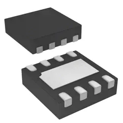
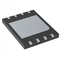
Images are for reference only
GD5F1GQ5REYIGR
IC FLASH 1GBIT SPI/QUAD
- Manufacturer
- Mfr. Part #GD5F1GQ5REYIGR
- Package
- Datasheet GD5F1GQ5REYIGR DataSheet
- In Stock28303
100% Original & New
24 Hours ready to ship
365 Days Warranty
RFQ & Get more Discounts
Specifications
| Series | GD5F |
| Part Status | Active |
| Memory Type | Non-Volatile |
| Memory Format | FLASH |
| Memory Size | 1Gbit |
| Memory Organization | 256M x 4 |
| Memory Interface | SPI - Quad I/O, QPI, DTR |
| Clock Frequency | 104 MHz |
| Voltage - Supply | 1.7V ~ 2V |
| Operating Temperature | -40°C ~ 85°C (TA) |
| Mounting Type | Surface Mount |
| Package / Case | 8-WDFN Exposed Pad |
| Base Product Number | GD5F1GQ5 |
| Technology | FLASH - NAND (SLC) |
| Write Cycle Time - Word, Page | 600µs |
| Supplier Device Package | 8-WSON (6x8) |
| Access Time | 9.5 ns |
Overview
Description
Features
1. Storage Capacity: Typically ranges from 120GB to 2TB, catering to various user needs.
2. Form Factor: Designed in the M.2 2280 format, making it compatible with modern laptops and desktops.
3. Interface: Utilizes the NVMe (Non-Volatile Memory Express) interface over PCIe, providing significantly faster data transfer rates compared to SATA SSDs.
4. Read/Write Speeds: Offers high sequential read/write speeds, often exceeding 3000 MB/s for reads and 2000 MB/s for writes, enhancing system responsiveness.
5. Endurance and Reliability: Built with advanced error correction and wear leveling technology, ensuring durability and longevity.
6. Thermal Management: Features built-in thermal throttling to prevent overheating during extensive use.
7. Low Power Consumption: Efficient power usage which is beneficial for battery-operated devices.
This SSD is ideal for gamers, content creators, and professionals seeking enhanced performance in data-intensive applications.
Package
Pinout
The primary functions of the pins include:
1. Data Input/Output: Several pins (D0 to D7) facilitate 8-bit data transfer.
2. Command Interface: Pins for commands and control signals, including Chip Enable (CE), Write Enable (WE), and Read Enable (RE).
3. Addressing: Address pins allow the device to access specific memory locations.
4. Power Supply: VCC and VSS pins provide power to the device.
5. Protection and Status: Additional pins handle device status and protection features.
The device supports various read, write, and erase functions necessary for NAND flash operations, making it suitable for applications requiring reliable non-volatile storage.
Manufacturer
Equivalent
Shipping
Shipping MethodsWe
offer global shipping services through DHL, FedEx, TNT, UPS, or any other forwarder of your choice.
Shipping Fee Reference (DHL/FedEx):
DHL: Shipping cost ranges from $25-$45 (0.5kg), with an estimated delivery time of 2-5 business days.
FedEx: Shipping cost ranges from $25-$40 (0.5kg), with an estimated delivery time of 3-7 business days.
UPS: Shipping cost ranges from $25-$45 (0.5kg), with an estimated delivery time of 3-7 business days.
TNT: Shipping cost ranges from $25-$65 (0.5kg), with an estimated delivery time of 3-7 business days.
EMS: Shipping cost ranges from $30-$50 (0.5kg), with an estimated delivery time of 7-15 business days.
Registered Air Mail: Shipping cost is $2-$4 (0.1kg), with an estimated delivery time of 5-20 business days.
Payments
Payment Methods
The Payment term is 100% Prepaid.
Currently, we only accept the below payment methods:
1. PayPal
2. Credit/ Debit Card
3. Wire Transfer
Similar
-
![MX29F400CBTI-70G]() MX29F400CBTI-70G
Macronix
-
![MX66U1G45GXDI00]() MX66U1G45GXDI00
Macronix
-
![MX25V4035FZUI]() MX25V4035FZUI
Macronix
-
![MX25V16066M2I02]() MX25V16066M2I02
Macronix
-
![MX25R6435FBDIL0]() MX25R6435FBDIL0
Macronix
-
![MX25U25643GZNI00]() MX25U25643GZNI00
Macronix
-
![MX25R1635FZUIH0]() MX25R1635FZUIH0
Macronix
-
![MX25V1635FM2I]() MX25V1635FM2I
Macronix
-
![MX25U3232FZBI02]() MX25U3232FZBI02
Macronix
-
![MX25L6433FM2I-08G]() MX25L6433FM2I-08G
Macronix
-
![MX25U6435FM2I-10G]() MX25U6435FM2I-10G
Macronix
-
![MX25L12833FZ2I-10G]() MX25L12833FZ2I-10..
Macronix