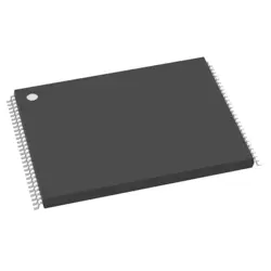
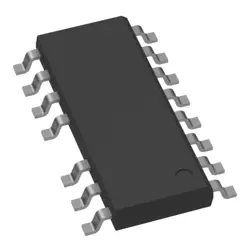
Images are for reference only
HCF4094BE
- Manufacturer
- Mfr. Part #HCF4094BE
- Package
- Datasheet
- In Stock6926
100% Original & New
24 Hours ready to ship
365 Days Warranty
RFQ & Get more Discounts
Specifications
| Manufacturer | STMicroelectronics |
| Package | DIP-16 |
Overview
Description
Key features include a serial data input, a clock input for data shifting, and a strobe input for latching the data. The device outputs include 8 parallel data outputs and a serial output for cascading additional registers. It operates with a wide supply voltage range from 3V to 15V, making it versatile for various electronic projects. The HCF4094BE is typically used in LED display drivers, digital data storage, and control systems where efficient data manipulation is required. The device is lauded for its low power consumption and high noise immunity, traits typical of CMOS technology.
Features
1. 8-Bit Shift Register and Latch: It combines an 8-bit shift register with a data latch and a 3-state output.
2. High-Speed Operation: The device can handle high-speed operations due to its fast switching characteristics.
3. Low Power Consumption: Being a CMOS device, it has low power consumption, making it suitable for battery-powered applications.
4. Wide Supply Voltage Range: It operates over a wide voltage range, typically from 3V to 15V, enhancing its versatility.
5. 3-State Outputs: The outputs can be set to high, low, or high-impedance states, allowing for bus interfacing.
6. Serial Input and Output: It supports serial data input and output, enabling easy cascading of multiple devices for extended data storage.
7. Latch Enable Input: It allows data to be latched, holding it for further processing or output.
These features make the HCF4094BE suitable for applications requiring serial-to-parallel conversion, data storage, and light control in low-power environments.
Package
Pinout
1. Pin 1 (Q1-Q7) - These are the parallel data output pins (Q1 to Q7) which output the stored data.
2. Pin 2 (Q7') - Serial data output, used for cascading multiple HCF4094BEs.
3. Pin 3 (CP) - Clock input, triggers the data shifting.
4. Pin 4 (STROBE) - Controls the output of the shift register.
5. Pin 5 (DI) - Serial data input, where the data is fed into the shift register.
6. Pin 6 (MR) - Master Reset, clears all data when activated.
7. Pin 7 (Q8/Q7') - Additional serial output used for cascading.
8. Pin 9 to 12, 15 - Outputs Q2 to Q6.
9. Pin 13 (G) - Output enable, activates the three-state outputs.
10. Pin 14 (VDD) - Positive power supply.
11. Pin 8 (VSS) - Ground.
The HCF4094BE is typically used in applications requiring serial data input and parallel data output, such as LED displays and other digital data storage interfaces.
Manufacturer
Application
Equivalent
Shipping
Shipping MethodsWe
offer global shipping services through DHL, FedEx, TNT, UPS, or any other forwarder of your choice.
Shipping Fee Reference (DHL/FedEx):
DHL: Shipping cost ranges from $25-$45 (0.5kg), with an estimated delivery time of 2-5 business days.
FedEx: Shipping cost ranges from $25-$40 (0.5kg), with an estimated delivery time of 3-7 business days.
UPS: Shipping cost ranges from $25-$45 (0.5kg), with an estimated delivery time of 3-7 business days.
TNT: Shipping cost ranges from $25-$65 (0.5kg), with an estimated delivery time of 3-7 business days.
EMS: Shipping cost ranges from $30-$50 (0.5kg), with an estimated delivery time of 7-15 business days.
Registered Air Mail: Shipping cost is $2-$4 (0.1kg), with an estimated delivery time of 5-20 business days.
Payments
Payment Methods
The Payment term is 100% Prepaid.
Currently, we only accept the below payment methods:
1. PayPal
2. Credit/ Debit Card
3. Wire Transfer
Similar
-
![MX25L3233FZBI-08Q]() MX25L3233FZBI-08Q
Macronix
-
![MX25L3233FM1I-08Q]() MX25L3233FM1I-08Q
Macronix
-
![MX25V16066M1I02]() MX25V16066M1I02
Macronix
-
![MX25L25673GMI-08G]() MX25L25673GMI-08G
Macronix
-
![MX25U25643GZNI00]() MX25U25643GZNI00
Macronix
-
![MX25L2006EM1I-12G]() MX25L2006EM1I-12G
Macronix
-
![MX25V1635FM2I]() MX25V1635FM2I
Macronix
-
![MX25L6433FM2I-08G]() MX25L6433FM2I-08G
Macronix
-
![MX25L12833FM2I-10G]() MX25L12833FM2I-10..
Macronix
-
![MX29LV160DTTI-70G]() MX29LV160DTTI-70G
Macronix
-
![MX25L25645GXDI-08G]() MX25L25645GXDI-08..
Macronix
-
![MX25L25735FMI-10G]() MX25L25735FMI-10G
Macronix