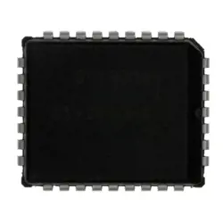
Images are for reference only
HMC491LP3ETR
IC AMP VSAT 3.4GHZ-3.8GHZ 16QFN
- Manufacturer
- Mfr. Part #HMC491LP3ETR
- Package 16-VFQFN Exposed Pad
- Datasheet HMC491LP3ETR DataSheet
- In Stock21528
100% Original & New
24 Hours ready to ship
365 Days Warranty
RFQ & Get more Discounts
Specifications
| Supplier | Analog Devices Inc. |
| Package | Tape & Reel (TR) |
| ProductStatus | Obsolete |
| Frequency | 3.4GHz ~ 3.8GHz |
| P1dB | 28dBm |
| Gain | 16dB |
| NoiseFigure | 2.2dB |
| RFType | VSAT |
| Voltage-Supply | 3V |
| Current-Supply | 9mA |
| TestFrequency | 3.8GHz |
| MountingType | Surface Mount |
| Package/Case | 16-VFQFN Exposed Pad |
Overview
Description
Key features include a low noise figure, high linearity, and a compact package, enabling efficient integration into various systems. The device typically operates with a single supply voltage, simplifying design and reducing overall system complexity. Its robust performance in challenging environments makes it suitable for a wide range of applications, including cellular, Wi-Fi, and satellite communications.
For detailed specifications, including gain, input and output return loss, and power consumption, refer to the manufacturer's datasheet.
Features
1. Gain: Provides a typical gain of 20 dB, allowing for efficient signal amplification.
2. Noise Figure: Low noise figure of around 3 dB ensures minimal signal degradation.
3. Output Power: Capable of delivering output power of +18 dBm, making it suitable for various transmission applications.
4. Supply Voltage: Operates on a supply voltage of +5V, facilitating easy integration into existing systems.
5. Package: Available in a compact 3 mm x 3 mm LFCSP (leadframe chip-scale package), optimizing space in circuit designs.
6. Application: Ideal for cellular, Wi-Fi, and other wireless communication applications.
These features combined make the HMC491LP3ETR a versatile choice for enhancing signal strength in various RF systems.
Package
Pinout
The primary functions of the pins include RF input and output, DC biasing, and ground connections. Key pins include:
- RF Input (Pin 1): Receives the input RF signal.
- RF Output (Pin 3): Outputs the amplified RF signal.
- Vdd (Pins 6, 12): Power supply connections for the amplifier's operation.
- GND (Pins 4, 5, 10, 11): Ground connections for stability and performance.
- Control pins (Pins 8, 9): Used for enabling/disabling the amplifier or controlling gain settings.
This device is optimized for operation in the frequency range of 1 to 12 GHz, making it suitable for applications such as radar, communications, and instrumentation.
Manufacturer
Application
Equivalent
Shipping
Shipping MethodsWe
offer global shipping services through DHL, FedEx, TNT, UPS, or any other forwarder of your choice.
Shipping Fee Reference (DHL/FedEx):
DHL: Shipping cost ranges from $25-$45 (0.5kg), with an estimated delivery time of 2-5 business days.
FedEx: Shipping cost ranges from $25-$40 (0.5kg), with an estimated delivery time of 3-7 business days.
UPS: Shipping cost ranges from $25-$45 (0.5kg), with an estimated delivery time of 3-7 business days.
TNT: Shipping cost ranges from $25-$65 (0.5kg), with an estimated delivery time of 3-7 business days.
EMS: Shipping cost ranges from $30-$50 (0.5kg), with an estimated delivery time of 7-15 business days.
Registered Air Mail: Shipping cost is $2-$4 (0.1kg), with an estimated delivery time of 5-20 business days.
Payments
Payment Methods
The Payment term is 100% Prepaid.
Currently, we only accept the below payment methods:
1. PayPal
2. Credit/ Debit Card
3. Wire Transfer
Similar
-
![MX25L3233FM1I-08Q]() MX25L3233FM1I-08Q
MX25L3233FM1I-08Q
Macronix
-
![MX29F400CBTI-70G]() MX29F400CBTI-70G
MX29F400CBTI-70G
Macronix
-
![MX66U1G45GXDI00]() MX66U1G45GXDI00
MX66U1G45GXDI00
Macronix
-
![MX25R3235FZNIL0]() MX25R3235FZNIL0
MX25R3235FZNIL0
Macronix
-
![MX25V16066M2I02]() MX25V16066M2I02
MX25V16066M2I02
Macronix
-
![MX25L8035EM2I-10G]() MX25L8035EM2I-10G
MX25L8035EM2I-10G
Macronix
-
![MX25R6435FBDIL0]() MX25R6435FBDIL0
MX25R6435FBDIL0
Macronix
-
![MX25U25643GZNI00]() MX25U25643GZNI00
MX25U25643GZNI00
Macronix
-
![MX25L2006EM1I-12G]() MX25L2006EM1I-12G
MX25L2006EM1I-12G
Macronix
-
![MX25V1635FM2I]() MX25V1635FM2I
MX25V1635FM2I
Macronix
-
![MX25U25645GXDI00]() MX25U25645GXDI00
MX25U25645GXDI00
Macronix
-
![MX29F040CQI-70G]() MX29F040CQI-70G
MX29F040CQI-70G
Macronix