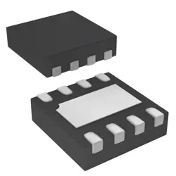
Images are for reference only
ICS8543BGILF
- Manufacturer
- Mfr. Part #ICS8543BGILF
- Package
- Datasheet ICS8543BGILF DataSheet
- In Stock4030
100% Original & New
24 Hours ready to ship
365 Days Warranty
RFQ & Get more Discounts
Specifications
| Manufacturer | RENESAS |
| Package | TSSOP-20 |
Overview
Description
Key features include a wide operating voltage range, low power consumption, and excellent signal integrity, which are critical for maintaining performance in demanding environments. The ICS8543BGILF is often used in conjunction with other clock management solutions to optimize system performance, especially in applications requiring precise timing controls like FPGAs, microcontrollers, and ASICs.
Additionally, its compact package and robust design make it ideal for space-constrained applications. Overall, the ICS8543BGILF is a versatile component for enhancing clock distribution in modern electronic systems.
Features
1. High-speed performance: Capable of supporting data rates up to 1.5 GHz.
2. Low skew: Ensures minimal propagation delay, enhancing timing accuracy across outputs.
3. Multiple outputs: Provides 3 differential outputs for signal distribution.
4. Single-ended and differential input: Allows flexibility in signal source configurations.
5. Wide power supply range: Operates typically from 3.3V to 5V, accommodating various system designs.
6. Low power consumption: Designed to minimize energy usage, contributing to overall system efficiency.
7. Thermal and ESD protection: Built to withstand environmental stresses, ensuring reliability in various applications.
8. Small package size: Available in a compact 16-pin TSSOP, suitable for space-constrained applications.
These features make the ICS8543BGILF ideal for telecom, datacom, and high-speed digital applications.
Package
Pinout
Pin Functions:
1. VDD (Power Supply): Powers the device.
2. GND (Ground): Ground connection.
3. CLK (Input): Differential clock input.
4. CLK (Input): Complementary differential clock input.
5. CLKOUT (Output): Buffered clock output.
6. CLKOUT (Output): Complementary buffered clock output.
7. S0-S2 (Select Pins): Used for selecting the output configuration.
8. OE (Output Enable): Activates or disables the output drivers.
9. NC (No Connect): Unconnected pin, not used.
10. VDD/VSS: Additional power supply and ground pins for stability.
This device is designed to enhance signal integrity and reduce skew for high-speed clock applications in digital systems.
Manufacturer
Application
Equivalent
Shipping
Shipping MethodsWe
offer global shipping services through DHL, FedEx, TNT, UPS, or any other forwarder of your choice.
Shipping Fee Reference (DHL/FedEx):
DHL: Shipping cost ranges from $25-$45 (0.5kg), with an estimated delivery time of 2-5 business days.
FedEx: Shipping cost ranges from $25-$40 (0.5kg), with an estimated delivery time of 3-7 business days.
UPS: Shipping cost ranges from $25-$45 (0.5kg), with an estimated delivery time of 3-7 business days.
TNT: Shipping cost ranges from $25-$65 (0.5kg), with an estimated delivery time of 3-7 business days.
EMS: Shipping cost ranges from $30-$50 (0.5kg), with an estimated delivery time of 7-15 business days.
Registered Air Mail: Shipping cost is $2-$4 (0.1kg), with an estimated delivery time of 5-20 business days.
Payments
Payment Methods
The Payment term is 100% Prepaid.
Currently, we only accept the below payment methods:
1. PayPal
2. Credit/ Debit Card
3. Wire Transfer
Similar
-
![MX25R8035FM1IL0]() MX25R8035FM1IL0
MX25R8035FM1IL0
Macronix
-
![MX25L3233FM1I-08Q]() MX25L3233FM1I-08Q
MX25L3233FM1I-08Q
Macronix
-
![MX25V1635FZNQ03]() MX25V1635FZNQ03
MX25V1635FZNQ03
Macronix
-
![MX25V16066M1I02]() MX25V16066M1I02
MX25V16066M1I02
Macronix
-
![MX25L25673GMI-10G]() MX25L25673GMI-10G
MX25L25673GMI-10G
Macronix
-
![MX29GL512FHXFI-11G]() MX29GL512FHXFI-11..
MX29GL512FHXFI-11..
Macronix
-
![MX25U25643GZNI00]() MX25U25643GZNI00
MX25U25643GZNI00
Macronix
-
![MX25L2006EM1I-12G]() MX25L2006EM1I-12G
MX25L2006EM1I-12G
Macronix
-
![MX25U3232FZBI02]() MX25U3232FZBI02
MX25U3232FZBI02
Macronix
-
![MX25L12833FM2I-10G]() MX25L12833FM2I-10..
MX25L12833FM2I-10..
Macronix
-
![MX25U25645GXDI00]() MX25U25645GXDI00
MX25U25645GXDI00
Macronix
-
![MX29LV160DTTI-70G]() MX29LV160DTTI-70G
MX29LV160DTTI-70G
Macronix