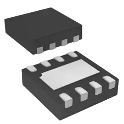
Images are for reference only
JFM29GL256RH
- Manufacturer
- Mfr. Part #JFM29GL256RH
- Package
- Datasheet
- In Stock3817
100% Original & New
24 Hours ready to ship
365 Days Warranty
RFQ & Get more Discounts
Specifications
| Manufacturer | JLCPCB Assembly |
| Package | TSOP-56 |
Overview
Description
Key features of the JFM29GL256RH include a 256 megabit storage capacity, organized in a block architecture for efficient data management. It supports a wide range of operating temperatures, making it suitable for various industrial applications. The chip provides fast read times, enhancing system performance, and supports standard interfaces for easy integration into existing systems.
The device is designed for reliability and endurance, with a high number of program/erase cycles, ensuring long-term data retention. It typically uses a standard parallel interface for communication, making it compatible with many microcontrollers and processors.
Overall, the JFM29GL256RH is a robust choice for applications requiring reliable, high-speed data storage and retrieval, especially in environments where durability and longevity are critical.
Features
1. Architecture: It utilizes NOR flash technology, offering fast read times and random access capability, making it suitable for executing code directly from the flash.
2. Interface: It supports a parallel interface, which allows for efficient data transfer and is compatible with various microcontrollers and processors.
3. Voltage Range: The device operates within a voltage range of 2.7V to 3.6V, making it compatible with standard system power supplies.
4. Performance: With a fast read access time typically around 90 ns, it ensures quick data retrieval and is optimal for systems requiring rapid access to firmware or software.
5. Sector Architecture: The memory is organized into uniform sectors, allowing for flexible erasing and programming capabilities, essential for applications needing regular updates.
6. Endurance and Reliability: It provides a high degree of data retention and endurance, typically offering 100,000 program/erase cycles per sector.
Overall, the JFM29GL256RH is designed for reliability and performance in embedded applications.
Package
Pinout
The device is often used in applications where data integrity and reliability are critical, such as embedded systems, consumer electronics, and industrial applications. The pins on the JFM29GL256RH are used for various functions, including power supply, ground, address inputs, data inputs/outputs, chip enable, write enable, output enable, and reset. The detailed pin configuration and specific functions should be referenced from the manufacturer’s datasheet for precise design and integration information.
Manufacturer
Application
Equivalent
Shipping
Shipping MethodsWe
offer global shipping services through DHL, FedEx, TNT, UPS, or any other forwarder of your choice.
Shipping Fee Reference (DHL/FedEx):
DHL: Shipping cost ranges from $25-$45 (0.5kg), with an estimated delivery time of 2-5 business days.
FedEx: Shipping cost ranges from $25-$40 (0.5kg), with an estimated delivery time of 3-7 business days.
UPS: Shipping cost ranges from $25-$45 (0.5kg), with an estimated delivery time of 3-7 business days.
TNT: Shipping cost ranges from $25-$65 (0.5kg), with an estimated delivery time of 3-7 business days.
EMS: Shipping cost ranges from $30-$50 (0.5kg), with an estimated delivery time of 7-15 business days.
Registered Air Mail: Shipping cost is $2-$4 (0.1kg), with an estimated delivery time of 5-20 business days.
Payments
Payment Methods
The Payment term is 100% Prepaid.
Currently, we only accept the below payment methods:
1. PayPal
2. Credit/ Debit Card
3. Wire Transfer
Similar
-
![MX25L3233FM1I-08Q]() MX25L3233FM1I-08Q
MX25L3233FM1I-08Q
Macronix
-
![MX25V1635FZNQ03]() MX25V1635FZNQ03
MX25V1635FZNQ03
Macronix
-
![MX66U1G45GXDI00]() MX66U1G45GXDI00
MX66U1G45GXDI00
Macronix
-
![MX25V2033FM1I]() MX25V2033FM1I
MX25V2033FM1I
Macronix
-
![MX30LF2G28AD-TI]() MX30LF2G28AD-TI
MX30LF2G28AD-TI
Macronix
-
![MX25L8035EM2I-10G]() MX25L8035EM2I-10G
MX25L8035EM2I-10G
Macronix
-
![MX25L25673GMI-08G]() MX25L25673GMI-08G
MX25L25673GMI-08G
Macronix
-
![MX25L25673GMI-10G]() MX25L25673GMI-10G
MX25L25673GMI-10G
Macronix
-
![MX25U51279GXDR00]() MX25U51279GXDR00
MX25U51279GXDR00
Macronix
-
![MX25U25643GZNI00]() MX25U25643GZNI00
MX25U25643GZNI00
Macronix
-
![MX25U3232FZBI02]() MX25U3232FZBI02
MX25U3232FZBI02
Macronix
-
![MX25L12833FM2I-10G]() MX25L12833FM2I-10..
MX25L12833FM2I-10..
Macronix