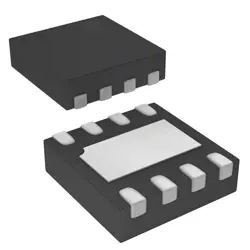
Images are for reference only
JS28F320C3TD70
IC FLSH 32MBIT PARALLEL 48TSOP I
- Manufacturer
- Mfr. Part #JS28F320C3TD70
- Package TSOP48
- Datasheet
- In Stock3627
100% Original & New
24 Hours ready to ship
365 Days Warranty
RFQ & Get more Discounts
Specifications
| Package | Tray |
| ProductStatus | Obsolete |
| MemoryType | Non-Volatile |
| MemoryFormat | FLASH |
| Technology | FLASH - Boot Block |
| MemorySize | 32Mb (2M x 16) |
| MemoryInterface | Parallel |
| WriteCycleTime-WordPage | 70ns |
| AccessTime | 70 ns |
| Voltage-Supply | 2.7V ~ 3.6V |
| OperatingTemperature | -40°C ~ 85°C (TA) |
| MountingType | Surface Mount |
| Package/Case | 48-TFSOP (0.724, 18.40mm Width) |
Overview
Description
Key features include:
- Interface: The chip typically uses a parallel interface, allowing for fast read and write operations.
- Memory Structure: It consists of multiple sectors, enabling efficient erasing and programming.
- Performance: It supports fast random access and high-speed read operations, which are crucial for performance-sensitive applications.
- Reliability: The chip is designed for endurance, with a typical write/erase cycle of up to 100,000 cycles and data retention of over 20 years.
Due to its compact size and efficiency, the JS28F320C3TD70 is a common choice for firmware storage in consumer electronics and other devices requiring reliable, quick access to stored data.
Features
- Memory Density: 32 Mb (4 MB) capacity.
- Access Time: Offers fast read access times, typically around 70 ns.
- Interface: Parallel interface with a standard 8-bit or 16-bit data bus.
- Voltage: Operates at a single 3.0V to 3.6V power supply.
- Endurance: Supports a high number of program/erase cycles, typically around 100,000 cycles per sector.
- Data Retention: Provides reliable data retention of up to 20 years.
- Sector Erase: Features sector-based erase capabilities, allowing for targeted data management.
- Compatible: Ideal for use in embedded systems, automotive applications, and consumer electronics.
This device is well-suited for applications requiring reliable, high-speed data storage with long-term retention.
Package
Pinout
### Pin Count:
- Total Pins: 48
### Key Functions:
- Data Input/Output Pins (DQ0-DQ7): 8 data lines for read and write operations.
- Address Lines (A0-A19): Used for selecting memory locations (20 address lines).
- Control Pins:
- WE# (Write Enable): Enables write operations.
- OE# (Output Enable): Enables output during read operations.
- CE# (Chip Enable): Activates the device for read/write.
- Vcc: Power supply pin.
- Vss: Ground pin.
- Reset Pin: Used to reset the memory device.
This device is commonly used in embedded systems for firmware storage due to its non-volatile characteristics.
Manufacturer
Application
Equivalent
Shipping
Shipping MethodsWe
offer global shipping services through DHL, FedEx, TNT, UPS, or any other forwarder of your choice.
Shipping Fee Reference (DHL/FedEx):
DHL: Shipping cost ranges from $25-$45 (0.5kg), with an estimated delivery time of 2-5 business days.
FedEx: Shipping cost ranges from $25-$40 (0.5kg), with an estimated delivery time of 3-7 business days.
UPS: Shipping cost ranges from $25-$45 (0.5kg), with an estimated delivery time of 3-7 business days.
TNT: Shipping cost ranges from $25-$65 (0.5kg), with an estimated delivery time of 3-7 business days.
EMS: Shipping cost ranges from $30-$50 (0.5kg), with an estimated delivery time of 7-15 business days.
Registered Air Mail: Shipping cost is $2-$4 (0.1kg), with an estimated delivery time of 5-20 business days.
Payments
Payment Methods
The Payment term is 100% Prepaid.
Currently, we only accept the below payment methods:
1. PayPal
2. Credit/ Debit Card
3. Wire Transfer
Similar
-
![MX25L3233FZBI-08Q]() MX25L3233FZBI-08Q
MX25L3233FZBI-08Q
Macronix
-
![MX25V2033FM1I]() MX25V2033FM1I
MX25V2033FM1I
Macronix
-
![MX25V16066M1I02]() MX25V16066M1I02
MX25V16066M1I02
Macronix
-
![MX30LF2G28AD-TI]() MX30LF2G28AD-TI
MX30LF2G28AD-TI
Macronix
-
![MX25L25673GMI-08G]() MX25L25673GMI-08G
MX25L25673GMI-08G
Macronix
-
![MX25U25643GZNI00]() MX25U25643GZNI00
MX25U25643GZNI00
Macronix
-
![MX25V1635FM2I]() MX25V1635FM2I
MX25V1635FM2I
Macronix
-
![MX25U3232FZBI02]() MX25U3232FZBI02
MX25U3232FZBI02
Macronix
-
![MX25U6435FM2I-10G]() MX25U6435FM2I-10G
MX25U6435FM2I-10G
Macronix
-
![MX25L12833FZNI-10G]() MX25L12833FZNI-10..
MX25L12833FZNI-10..
Macronix
-
![MX29F040CTI-70G]() MX29F040CTI-70G
MX29F040CTI-70G
Macronix
-
![MX29LV640ETTI-70G]() MX29LV640ETTI-70G
MX29LV640ETTI-70G
Macronix