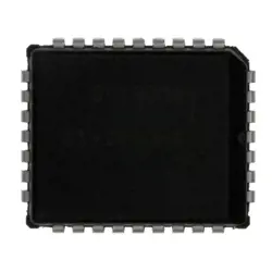
Images are for reference only
K4FBE3D4HM-TFCL
32Gbit 2.133GHz LPDDR4 SDRAM FBGA-200 Memory (ICs) RoHS
- Manufacturer
- Mfr. Part #K4FBE3D4HM-TFCL
- Package
- Datasheet K4FBE3D4HM-TFCL DataSheet
- In Stock13970
100% Original & New
24 Hours ready to ship
365 Days Warranty
RFQ & Get more Discounts
Specifications
| Packaging | FBGA-200 |
| Clock Frequency | 2.133GHz |
| Current - Supply | 12mA |
| Memory Format | LPDDR4 SDRAM |
| Memory Size | 32Gbit |
| Operating temperature | -40℃~+95℃ |
| Refresh Current | 2mA |
| Voltage - Supply | 1.06V~1.17V;1.7V~1.95V |
Overview
Description
The TFCL designation indicates features such as the use of advanced technology for improved density and power efficiency. It supports various storage capacities and interfaces, which allows for flexibility in design and integration into different systems. As part of Samsung's portfolio of memory solutions, K4FBE3D4HM-TFCL contributes to the overall performance and functionality of modern digital devices, catering to the growing demand for high-speed and high-capacity storage solutions.
Features
Key features include:
1. Capacity: Typically available in various densities, commonly 4GB to 8GB.
2. Speed: Supports high data rates, usually up to 3200 MT/s, enhancing overall system performance.
3. Power Efficiency: Designed for low power consumption, making it ideal for battery-operated devices.
4. Wide I/O Interface: Offers a wide I/O configuration to improve bandwidth.
5. Package Type: Comes in a compact package suitable for mobile applications, facilitating space-saving designs.
6. Thermal Performance: Developed to withstand varying thermal conditions while ensuring stable operation.
This chip is particularly suitable for smartphones, tablets, and other portable electronics, optimizing both speed and power usage.
Package
Pinout
The pin configuration includes power supply pins (VDD, VSS), data input/output pins (DQ), address input pins (A), control pins (CS, RAS, CAS, WE), and other supplementary pins for functionality like clock signals. The design and layout of these pins are crucial for ensuring proper communication and operation within a memory subsystem.
Manufacturer
Application
Equivalent
Shipping
Shipping MethodsWe
offer global shipping services through DHL, FedEx, TNT, UPS, or any other forwarder of your choice.
Shipping Fee Reference (DHL/FedEx):
DHL: Shipping cost ranges from $25-$45 (0.5kg), with an estimated delivery time of 2-5 business days.
FedEx: Shipping cost ranges from $25-$40 (0.5kg), with an estimated delivery time of 3-7 business days.
UPS: Shipping cost ranges from $25-$45 (0.5kg), with an estimated delivery time of 3-7 business days.
TNT: Shipping cost ranges from $25-$65 (0.5kg), with an estimated delivery time of 3-7 business days.
EMS: Shipping cost ranges from $30-$50 (0.5kg), with an estimated delivery time of 7-15 business days.
Registered Air Mail: Shipping cost is $2-$4 (0.1kg), with an estimated delivery time of 5-20 business days.
Payments
Payment Methods
The Payment term is 100% Prepaid.
Currently, we only accept the below payment methods:
1. PayPal
2. Credit/ Debit Card
3. Wire Transfer
Similar
-
![MX25R8035FM1IL0]() MX25R8035FM1IL0
MX25R8035FM1IL0
Macronix
-
![MX25L3233FZBI-08Q]() MX25L3233FZBI-08Q
MX25L3233FZBI-08Q
Macronix
-
![MX29F400CBTI-70G]() MX29F400CBTI-70G
MX29F400CBTI-70G
Macronix
-
![MX25V4035FZUI]() MX25V4035FZUI
MX25V4035FZUI
Macronix
-
![MX25V2033FM1I]() MX25V2033FM1I
MX25V2033FM1I
Macronix
-
![MX25R3235FZNIL0]() MX25R3235FZNIL0
MX25R3235FZNIL0
Macronix
-
![MX25L6433FM2I-08G]() MX25L6433FM2I-08G
MX25L6433FM2I-08G
Macronix
-
![MX25L12833FZ2I-10G]() MX25L12833FZ2I-10..
MX25L12833FZ2I-10..
Macronix
-
![MX25U25645GXDI00]() MX25U25645GXDI00
MX25U25645GXDI00
Macronix
-
![MX29LV160DTTI-70G]() MX29LV160DTTI-70G
MX29LV160DTTI-70G
Macronix
-
![MX29F040CQI-70G]() MX29F040CQI-70G
MX29F040CQI-70G
Macronix
-
![MX30LF4G18AC-TI]() MX30LF4G18AC-TI
MX30LF4G18AC-TI
Macronix