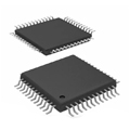
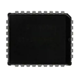
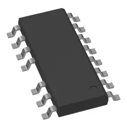
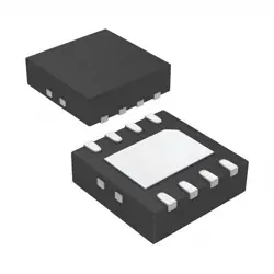
Images are for reference only
LTC1597ACG
Digital to Analog Converters - DAC LTC1597 - 16-Bit Parallel Low Glitch Multiplying DAC with 4-Quadrant Resistors
- Manufacturer
- Mfr. Part #LTC1597ACG
- Package
- Datasheet LTC1597ACG DataSheet
- In Stock18206
100% Original & New
24 Hours ready to ship
365 Days Warranty
RFQ & Get more Discounts
Specifications
Overview
Description
Key features include low power consumption (approximately 30 mW), differential input for improved noise performance, and a wide operating temperature range. The LTC1597ACG also includes built-in sample-and-hold circuitry, which aids in capturing fast-changing signals accurately. Its compact 28-lead SSOP package allows for space-efficient designs in various applications, including portable instrumentation and industrial automation. Overall, the LTC1597ACG is an excellent choice for engineers seeking a high-performance ADC for demanding applications.
Features
1. Speed: It operates at a maximum conversion rate of 1 MSPS (million samples per second).
2. Resolution: Offers 12-bit resolution, providing a high level of detail in signal conversion.
3. Input Voltage Range: It supports a single-ended input voltage range of 0V to 5V.
4. Low Power: Consumes only 15 mW in normal operation, making it suitable for battery-powered devices.
5. Differential Inputs: Can accept differential input signals to reduce noise.
6. Built-In Sample-and-Hold: Features an integrated sample-and-hold circuit for improved signal accuracy.
7. Serial Interface: Communicates via a serial interface for easy integration with microcontrollers and digital processors.
8. Temperature Range: Operates effectively over an extended temperature range, enhancing reliability in various environments.
These features make the LTC1597ACG ideal for applications in instrumentation, audio processing, and other high-speed data acquisition systems.
Package
Pinout
### Pin Functions:
1. VDD: Power supply.
2. VSS: Ground reference.
3. REF: Reference voltage input for the ADC.
4. AIN: Analog input for conversion.
5. BUSY: Indicates when the ADC is converting.
6. CS: Chip select for enabling the device.
7. RD: Read strobe signal for data output.
8. WR: Write strobe for initiating the conversion.
9. CLK: Clock input for timing control.
10. D0-D7: Data output lines (8 bits).
11. AGND: Analog ground.
12. SYNC: Synchronization input for multiple ADCs.
The LTC1597ACG is designed for applications requiring precise analog signal conversion, typically in measurement and control systems.
Manufacturer
Application
Equivalent
Shipping
Shipping MethodsWe
offer global shipping services through DHL, FedEx, TNT, UPS, or any other forwarder of your choice.
Shipping Fee Reference (DHL/FedEx):
DHL: Shipping cost ranges from $25-$45 (0.5kg), with an estimated delivery time of 2-5 business days.
FedEx: Shipping cost ranges from $25-$40 (0.5kg), with an estimated delivery time of 3-7 business days.
UPS: Shipping cost ranges from $25-$45 (0.5kg), with an estimated delivery time of 3-7 business days.
TNT: Shipping cost ranges from $25-$65 (0.5kg), with an estimated delivery time of 3-7 business days.
EMS: Shipping cost ranges from $30-$50 (0.5kg), with an estimated delivery time of 7-15 business days.
Registered Air Mail: Shipping cost is $2-$4 (0.1kg), with an estimated delivery time of 5-20 business days.
Payments
Payment Methods
The Payment term is 100% Prepaid.
Currently, we only accept the below payment methods:
1. PayPal
2. Credit/ Debit Card
3. Wire Transfer
Similar
-
![MX25L3233FZBI-08Q]() MX25L3233FZBI-08Q
Macronix
-
![MX25V1635FZNQ03]() MX25V1635FZNQ03
Macronix
-
![MX29F400CBTI-70G]() MX29F400CBTI-70G
Macronix
-
![MX30LF2G28AD-TI]() MX30LF2G28AD-TI
Macronix
-
![MX25L8035EM2I-10G]() MX25L8035EM2I-10G
Macronix
-
![MX25L25673GMI-10G]() MX25L25673GMI-10G
Macronix
-
![MX25U25645GXDI00]() MX25U25645GXDI00
Macronix
-
![MX29F040CQI-70G]() MX29F040CQI-70G
Macronix
-
![MX25L25645GXDI-08G]() MX25L25645GXDI-08..
Macronix
-
![MX25L25735FMI-10G]() MX25L25735FMI-10G
Macronix
-
![MX25U51245GZ4I00]() MX25U51245GZ4I00
Macronix
-
![MX25L1006EMI-10G]() MX25L1006EMI-10G
Macronix