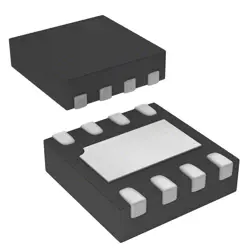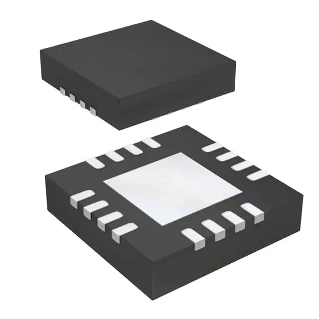
Images are for reference only
LTC6560HUD#PBF
IC TRANSIMPEDANCE AMP 16QFN
- Manufacturer
- Mfr. Part #LTC6560HUD#PBF
- Package QFN-16
- Datasheet LTC6560HUD#PBF DataSheet
- In Stock2435
100% Original & New
24 Hours ready to ship
365 Days Warranty
RFQ & Get more Discounts
Specifications
| Package | Tube |
| ProductStatus | Active |
| Type | Transimpedance Amplifier |
| Applications | LIDAR, Industrial Imaging |
| MountingType | Surface Mount |
| Package/Case | 16-WFQFN Exposed Pad |
Overview
Description
Key specifications include a gain bandwidth product of 1.2 GHz and a slew rate of 1600 V/μs, which allows it to handle fast-changing signals effectively. The device operates from a single or dual power supply, with a typical supply voltage range of ±2.5V to ±5V. It is housed in a compact 8-lead MSOP package, optimizing space in circuit designs.
Common applications include data acquisition systems, high-speed analog-to-digital converters (ADCs), and RF amplification. Overall, the LTC6560 is a versatile choice for engineers seeking high-performance amplification in demanding applications.
Features
1. Wide Bandwidth: The amplifier offers a high gain bandwidth of 185 MHz, making it suitable for fast signal processing.
2. Low Noise: It has a low input voltage noise density of 2.5 nV/√Hz, ensuring high fidelity in signal amplification.
3. High Common Mode Rejection Ratio (CMRR): The CMRR is 100 dB at a gain of 10, which helps in rejecting common-mode signals.
4. Programmable Gain: The gain can be set from 1 to 1000 using external resistors, providing flexibility for various applications.
5. Low Total Harmonic Distortion (THD): THD is typically around 0.0005%, ensuring minimal signal distortion.
6. Single Supply Operation: It operates from a single supply voltage of 3 V to 12 V, simplifying power supply requirements.
7. Rail-to-Rail Output: The output can swing to the supply rails, maximizing dynamic range.
These features make the LTC6560HUD#PBF ideal for medical imaging, sensor signal conditioning, and high-performance data acquisition systems.
Package
Pinout
1. V+ (Pin 1): Supply voltage input.
2. V- (Pin 2): Negative supply voltage input.
3. IN+ (Pin 3): Positive input for the differential signal.
4. IN- (Pin 4): Negative input for the differential signal.
5. OUT (Pin 5): Output, which provides a single-ended signal based on the comparison.
6. NC (Pin 6): No connection, not used.
7. GND (Pin 7): Ground reference.
8. COMP (Pin 8): Compensation pin for stability.
The LTC6560 is designed for high-speed applications, offering low propagation delay and high bandwidth, making it suitable for high-frequency signal processing.
Manufacturer
Application
Equivalent
Shipping
Shipping MethodsWe
offer global shipping services through DHL, FedEx, TNT, UPS, or any other forwarder of your choice.
Shipping Fee Reference (DHL/FedEx):
DHL: Shipping cost ranges from $25-$45 (0.5kg), with an estimated delivery time of 2-5 business days.
FedEx: Shipping cost ranges from $25-$40 (0.5kg), with an estimated delivery time of 3-7 business days.
UPS: Shipping cost ranges from $25-$45 (0.5kg), with an estimated delivery time of 3-7 business days.
TNT: Shipping cost ranges from $25-$65 (0.5kg), with an estimated delivery time of 3-7 business days.
EMS: Shipping cost ranges from $30-$50 (0.5kg), with an estimated delivery time of 7-15 business days.
Registered Air Mail: Shipping cost is $2-$4 (0.1kg), with an estimated delivery time of 5-20 business days.
Payments
Payment Methods
The Payment term is 100% Prepaid.
Currently, we only accept the below payment methods:
1. PayPal
2. Credit/ Debit Card
3. Wire Transfer
Similar
-
![MX25R8035FM1IL0]() MX25R8035FM1IL0
Macronix
-
![MX25L3233FZBI-08Q]() MX25L3233FZBI-08Q
Macronix
-
![MX25L3233FM1I-08Q]() MX25L3233FM1I-08Q
Macronix
-
![MX66U1G45GXDI00]() MX66U1G45GXDI00
Macronix
-
![MX25V4035FZUI]() MX25V4035FZUI
Macronix
-
![MX25V2033FM1I]() MX25V2033FM1I
Macronix
-
![MX25V16066M2I02]() MX25V16066M2I02
Macronix
-
![MX30LF2G28AD-TI]() MX30LF2G28AD-TI
Macronix
-
![MX25L25673GMI-10G]() MX25L25673GMI-10G
Macronix
-
![MX25V1635FM2I]() MX25V1635FM2I
Macronix
-
![MX25U3232FZBI02]() MX25U3232FZBI02
Macronix
-
![MX25U6435FM2I-10G]() MX25U6435FM2I-10G
Macronix