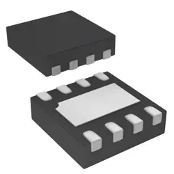
Images are for reference only
M25P40-VMN6TPB
4Mbit 2.3V~3.6V 75MHz SPI SO-8 Memory (ICs) RoHS
- Manufacturer
- Mfr. Part #M25P40-VMN6TPB
- Package
- Datasheet M25P40-VMN6TPB DataSheet
- In Stock8184
100% Original & New
24 Hours ready to ship
365 Days Warranty
RFQ & Get more Discounts
Specifications
| Packaging | SO-8 |
| Clock Frequency | 75MHz |
| Interface | SPI |
| Memory Size | 4Mbit |
| Operating temperature | -40℃~+85℃ |
| Voltage - Supply | 2.3V~3.6V |
| Data Retention - TDR (Year) | 20 Years |
| Page Programming Time (Tpp) | 800us |
| Program / Erase Cycles | 100,000 cycles |
| Standby Supply Current | 1uA |
| Write Cycle Time(tWC) | 5ms |
Overview
Description
Key features include a wide operating voltage range (typically 2.7V to 3.6V), low power consumption, and a robust endurance rating of up to 100,000 write/erase cycles. The chip supports various commands for program, erase, and read operations, making it versatile for different applications. Additionally, it comes in a compact SO-8 package, suitable for space-constrained designs. Its reliability and efficiency make the M25P40-VMN6TPB an ideal choice for applications requiring non-volatile memory solutions.
Features
1. Interface: Utilizes a Serial Peripheral Interface (SPI) for simple connectivity and fast data transfer.
2. Speed: Supports a maximum clock frequency of 104 MHz, enabling quick read and program operations.
3. Density: Offers 4 Mb of storage capacity, suitable for firmware and data storage in compact applications.
4. Erase Capability: Supports sector and chip erase operations, allowing flexible memory management.
5. Voltage Range: Operates within a supply voltage range of 2.7V to 3.6V, making it compatible with various embedded systems.
6. Data Retention: Provides a data retention period of up to 20 years, ensuring long-term data integrity.
7. Temperature Range: Rated for commercial temperature ranges of -40°C to 85°C, suitable for diverse operating environments.
8. Package Type: Available in a variety of packages, including 8-pin SOIC and other compact forms for efficient space utilization.
These features make the M25P40-VMN6TPB suitable for applications such as consumer electronics, automotive, and industrial devices.
Package
Pinout
1. SO (Serial Out): Data output pin.
2. SI (Serial In): Data input pin.
3. SCK (Serial Clock): Clock input pin.
4. CS (Chip Select): Active low pin for selecting the device.
5. VCC: Power supply (typically 2.7V to 3.6V).
6. GND: Ground reference.
7. WP (Write Protect): Write protection control pin (active low).
8. HD (Hold): Used to hold the device in a low-power mode.
The M25P40 supports SPI (Serial Peripheral Interface) communication, allowing for efficient data transfer and programming operations.
Manufacturer
Application
Equivalent
Shipping
Shipping MethodsWe
offer global shipping services through DHL, FedEx, TNT, UPS, or any other forwarder of your choice.
Shipping Fee Reference (DHL/FedEx):
DHL: Shipping cost ranges from $25-$45 (0.5kg), with an estimated delivery time of 2-5 business days.
FedEx: Shipping cost ranges from $25-$40 (0.5kg), with an estimated delivery time of 3-7 business days.
UPS: Shipping cost ranges from $25-$45 (0.5kg), with an estimated delivery time of 3-7 business days.
TNT: Shipping cost ranges from $25-$65 (0.5kg), with an estimated delivery time of 3-7 business days.
EMS: Shipping cost ranges from $30-$50 (0.5kg), with an estimated delivery time of 7-15 business days.
Registered Air Mail: Shipping cost is $2-$4 (0.1kg), with an estimated delivery time of 5-20 business days.
Payments
Payment Methods
The Payment term is 100% Prepaid.
Currently, we only accept the below payment methods:
1. PayPal
2. Credit/ Debit Card
3. Wire Transfer
Similar
-
![MX25R8035FM1IL0]() MX25R8035FM1IL0
MX25R8035FM1IL0
Macronix
-
![MX25V5126FM1I]() MX25V5126FM1I
MX25V5126FM1I
Macronix
-
![MX25V4035FZUI]() MX25V4035FZUI
MX25V4035FZUI
Macronix
-
![MX30LF2G28AD-TI]() MX30LF2G28AD-TI
MX30LF2G28AD-TI
Macronix
-
![MX25R6435FBDIL0]() MX25R6435FBDIL0
MX25R6435FBDIL0
Macronix
-
![MX25L25673GMI-10G]() MX25L25673GMI-10G
MX25L25673GMI-10G
Macronix
-
![MX25U51279GXDR00]() MX25U51279GXDR00
MX25U51279GXDR00
Macronix
-
![MX25L2006EM1I-12G]() MX25L2006EM1I-12G
MX25L2006EM1I-12G
Macronix
-
![MX25R1635FZUIH0]() MX25R1635FZUIH0
MX25R1635FZUIH0
Macronix
-
![MX25V1635FM2I]() MX25V1635FM2I
MX25V1635FM2I
Macronix
-
![MX25U3232FZBI02]() MX25U3232FZBI02
MX25U3232FZBI02
Macronix
-
![MX25U6435FM2I-10G]() MX25U6435FM2I-10G
MX25U6435FM2I-10G
Macronix