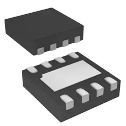
Images are for reference only
M25P80-VMN6TP
2.7V~3.6V 8Mbit 75MHz SPI SOIC-8 Memory (ICs) RoHS
- Manufacturer
- Mfr. Part #M25P80-VMN6TP
- Package
- Datasheet M25P80-VMN6TP DataSheet
- In Stock16983
100% Original & New
24 Hours ready to ship
365 Days Warranty
RFQ & Get more Discounts
Specifications
| Packaging | SOIC-8 |
| Clock Frequency | 75MHz |
| Interface | SPI |
| Memory Size | 8Mbit |
| Voltage - Supply | 2.7V~3.6V |
| Data Retention - TDR (Year) | 20 Years |
| Page Programming Time (Tpp) | 640us |
| Program / Erase Cycles | 100,000 cycles |
Overview
Description
Key features include a read speed of up to 25 MHz, multiple read modes (including dual and quad SPI), and a uniform sector architecture, allowing for efficient data management and erasure. The M25P80 is commonly used in embedded systems, consumer electronics, and automotive applications where reliable data storage is crucial.
It also supports various commands for reading, writing, and erasing data, along with features such as write protection and a deep power-down mode for energy conservation. Overall, the M25P80-VMN6TP is a versatile memory solution for applications requiring compact and efficient data storage.
Features
1. Interface: SPI (Serial Peripheral Interface) for easy integration with microcontrollers and other devices.
2. Operating Voltage: Typically ranges from 2.7V to 3.6V for flexibility in various applications.
3. Speed: Supports clock frequencies up to 66 MHz, allowing for fast data access.
4. Data Retention: Provides a minimum of 20 years of data retention at 85°C.
5. Endurance: Supports 10,000 program/erase cycles, ensuring durability for frequent write operations.
6. Package: Available in an 8-pin SOIC package, suitable for compact designs.
7. Commands: Supports standard commands for read, program, erase, and write operations.
8. Low Power Consumption: Designed for low power usage, making it suitable for battery-operated devices.
These features make the M25P80-VMN6TP ideal for applications in consumer electronics, industrial automation, and automotive systems.
Package
Pinout
The pin functions are as follows:
1. CS# (Chip Select): Active low pin used to select the device.
2. SCK (Serial Clock): The clock input for serial communication.
3. SI (Serial Input): Data input pin for commands and data.
4. SO (Serial Output): Data output pin for reading data.
5. WP# (Write Protect): Active low pin to protect the memory from being written.
6. HOLD# (Hold): Active low pin to pause operations without deselecting the device.
7. VCC: Power supply pin (typically 2.7V to 3.6V).
8. GND: Ground reference pin.
This device supports various modes of operation and features such as a dual/quad I/O interface for higher data transfer rates.
Manufacturer
Application
Equivalent
Shipping
Shipping MethodsWe
offer global shipping services through DHL, FedEx, TNT, UPS, or any other forwarder of your choice.
Shipping Fee Reference (DHL/FedEx):
DHL: Shipping cost ranges from $25-$45 (0.5kg), with an estimated delivery time of 2-5 business days.
FedEx: Shipping cost ranges from $25-$40 (0.5kg), with an estimated delivery time of 3-7 business days.
UPS: Shipping cost ranges from $25-$45 (0.5kg), with an estimated delivery time of 3-7 business days.
TNT: Shipping cost ranges from $25-$65 (0.5kg), with an estimated delivery time of 3-7 business days.
EMS: Shipping cost ranges from $30-$50 (0.5kg), with an estimated delivery time of 7-15 business days.
Registered Air Mail: Shipping cost is $2-$4 (0.1kg), with an estimated delivery time of 5-20 business days.
Payments
Payment Methods
The Payment term is 100% Prepaid.
Currently, we only accept the below payment methods:
1. PayPal
2. Credit/ Debit Card
3. Wire Transfer
Similar
-
![MX25L3233FZBI-08Q]() MX25L3233FZBI-08Q
MX25L3233FZBI-08Q
Macronix
-
![MX66U1G45GXDI00]() MX66U1G45GXDI00
MX66U1G45GXDI00
Macronix
-
![MX25V16066M1I02]() MX25V16066M1I02
MX25V16066M1I02
Macronix
-
![MX25V16066M2I02]() MX25V16066M2I02
MX25V16066M2I02
Macronix
-
![MX25L8035EM2I-10G]() MX25L8035EM2I-10G
MX25L8035EM2I-10G
Macronix
-
![MX25L25673GMI-08G]() MX25L25673GMI-08G
MX25L25673GMI-08G
Macronix
-
![MX25L2006EM1I-12G]() MX25L2006EM1I-12G
MX25L2006EM1I-12G
Macronix
-
![MX25R1635FZUIH0]() MX25R1635FZUIH0
MX25R1635FZUIH0
Macronix
-
![MX25U3232FZBI02]() MX25U3232FZBI02
MX25U3232FZBI02
Macronix
-
![MX25L6433FM2I-08G]() MX25L6433FM2I-08G
MX25L6433FM2I-08G
Macronix
-
![MX25U6435FM2I-10G]() MX25U6435FM2I-10G
MX25U6435FM2I-10G
Macronix
-
![MX25L12833FM2I-10G]() MX25L12833FM2I-10..
MX25L12833FM2I-10..
Macronix