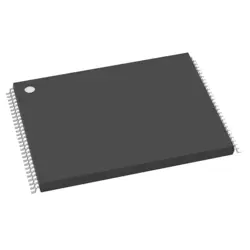
Images are for reference only
M27C1001-12F1
IC EPROM 1MBIT PARALLEL 32CDIP
- Manufacturer
- Mfr. Part #M27C1001-12F1
- Package FDIP-32W
- Datasheet
- In Stock2447
100% Original & New
24 Hours ready to ship
365 Days Warranty
RFQ & Get more Discounts
Specifications
| Package | Tube |
| ProductStatus | Obsolete |
| MemoryType | Non-Volatile |
| MemoryFormat | EPROM |
| Technology | EPROM - UV |
| MemorySize | 1Mb (128K x 8) |
| MemoryInterface | Parallel |
| AccessTime | 120 ns |
| Voltage-Supply | 4.5V ~ 5.5V |
| OperatingTemperature | 0°C ~ 70°C (TA) |
| MountingType | Through Hole |
| Package/Case | 32-CDIP (0.600, 15.24mm) Window |
Overview
Description
Key features include a single 5V power supply, low power consumption, and the ability to be erased using UV light, enabling reuse after programming. The M27C1001-12F1 is often used in applications like firmware storage, embedded systems, and situations requiring non-volatile memory.
It comes in various package types, including DIP and PLCC, facilitating integration into various electronic designs. The device’s programming and erasing processes require specific equipment, typically a programmer capable of handling EPROMs. Overall, the M27C1001-12F1 plays a crucial role in legacy systems and certain applications where reprogrammability is essential.
Features
1. Memory Organization: 128K x 8 bits.
2. Voltage Range: Operates typically between 4.5V to 5.5V.
3. High Speed: Access time of 12 ns, suitable for high-performance applications.
4. Reprogrammable: Can be erased using ultraviolet light, allowing for multiple programming cycles.
5. Low Power Consumption: Designed for low active and standby power consumption.
6. Reliability: Enhanced data retention and endurance capabilities.
7. Data Security: Offers options for data protection against unintentional writes.
8. Compatibility: Standard 32-pin DIP package, making it compatible with various memory circuits.
These features make the M27C1001-12F1 suitable for various applications including embedded systems, firmware storage, and prototyping.
Package
Pinout
The functions of its pins are as follows:
1. Address Pins (A0-A16): 17 address pins for accessing memory locations.
2. Data Pins (D0-D7): 8 data pins for data output.
3. Chip Enable (CE): Activates the chip for reading or programming.
4. Output Enable (OE): Controls data output when the chip is enabled.
5. Program Enable (PE): Activates programming mode.
6. Bulk Erase (BULK): Used for bulk erasure of the chip.
7. Vpp: Programming voltage pin (typically around 12.5V).
8. Vcc: Supply voltage pin (typically +5V).
9. Ground (GND): Common ground pin.
This configuration allows the M27C1001-12F1 to function effectively in read and programming operations.
Manufacturer
Application
Equivalent
Shipping
Shipping MethodsWe
offer global shipping services through DHL, FedEx, TNT, UPS, or any other forwarder of your choice.
Shipping Fee Reference (DHL/FedEx):
DHL: Shipping cost ranges from $25-$45 (0.5kg), with an estimated delivery time of 2-5 business days.
FedEx: Shipping cost ranges from $25-$40 (0.5kg), with an estimated delivery time of 3-7 business days.
UPS: Shipping cost ranges from $25-$45 (0.5kg), with an estimated delivery time of 3-7 business days.
TNT: Shipping cost ranges from $25-$65 (0.5kg), with an estimated delivery time of 3-7 business days.
EMS: Shipping cost ranges from $30-$50 (0.5kg), with an estimated delivery time of 7-15 business days.
Registered Air Mail: Shipping cost is $2-$4 (0.1kg), with an estimated delivery time of 5-20 business days.
Payments
Payment Methods
The Payment term is 100% Prepaid.
Currently, we only accept the below payment methods:
1. PayPal
2. Credit/ Debit Card
3. Wire Transfer
Similar
-
![MX25L3233FZBI-08Q]() MX25L3233FZBI-08Q
Macronix
-
![MX25V1635FZNQ03]() MX25V1635FZNQ03
Macronix
-
![MX25R3235FZNIL0]() MX25R3235FZNIL0
Macronix
-
![MX25R6435FBDIL0]() MX25R6435FBDIL0
Macronix
-
![MX29GL512FHXFI-11G]() MX29GL512FHXFI-11..
Macronix
-
![MX25U51279GXDR00]() MX25U51279GXDR00
Macronix
-
![MX25R1635FZUIH0]() MX25R1635FZUIH0
Macronix
-
![MX25L12833FZNI-10G]() MX25L12833FZNI-10..
Macronix
-
![MX25L12835FZ2I-10G]() MX25L12835FZ2I-10..
Macronix
-
![MX29LV160DTTI-70G]() MX29LV160DTTI-70G
Macronix
-
![MX29F040CTI-70G]() MX29F040CTI-70G
Macronix
-
![MX30LF4G18AC-TI]() MX30LF4G18AC-TI
Macronix