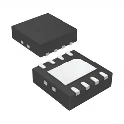

Images are for reference only
MAX4649EKA
Analog Switch ICs
- Manufacturer
- Mfr. Part #MAX4649EKA
- Package
- Datasheet
- In Stock26314
100% Original & New
24 Hours ready to ship
365 Days Warranty
RFQ & Get more Discounts
Specifications
Overview
Description
Key specifications include a typical on-resistance of approximately 0.5 ohms at 5V, fast switching times, and low crosstalk, which contribute to its effectiveness in high-frequency applications. The MAX4649EKA is housed in a compact, 8-pin µMAX package, facilitating easy integration into space-constrained designs.
This analog switch is particularly suitable for portable devices, consumer electronics, and industrial applications, where battery efficiency and signal integrity are paramount. Overall, the MAX4649EKA provides reliable performance and flexibility for engineers designing advanced electronic systems.
Features
1. Low On-Resistance: Typically 0.5Ω, ensuring minimal signal distortion.
2. Wide Voltage Range: Operates from a single supply of 2.7V to 12V and dual supplies ±2.7V to ±6V.
3. High Bandwidth: Supports analog signals with a bandwidth of up to 100MHz, making it suitable for RF applications.
4. Fast Switching Time: Rise and fall times are typically 8ns, allowing for rapid signal routing.
5. Low Power Consumption: Consumes only 2.5μA of supply current in off state, enhancing battery life in portable applications.
6. Logic-Compatible Control: Can be controlled by standard logic levels, simplifying integration with microcontrollers.
7. Ease of Use: Comes in a compact 16-Pin TQFN package, suitable for space-constrained designs.
These features make the MAX4649EKA ideal for applications in data acquisition, video switching, and signal routing.
Package
Pinout
The primary functions of the pins are as follows:
1. V+ (Pin 1): Positive supply voltage.
2. GND (Pin 8): Ground.
3. S1, S2 (Pins 2, 3, 5, 6): Signal inputs/outputs for the switches.
4. D1, D2 (Pins 4, 7): Common terminals for the switches.
5. IN1, IN2 (Pins 10, 11): Control inputs for switching operation.
6. COM (Pins 12, 13): Common nodes for the SPST switches.
7. NC (Pins 9, 14): No connect (not internally bonded).
8. EP (Pin 16): Exposed pad for thermal and mechanical grounding.
The device operates with low on-resistance and provides high-speed switching capabilities, making it suitable for various analog signal routing applications.
Manufacturer
Application
Equivalent
1. TSX01 - Texas Instruments
2. LMV324 - Texas Instruments
3. AD8495 - Analog Devices
4. OPA2134 - Texas Instruments
Ensure to verify specifications such as voltage range, bandwidth, and package type before substitution.
Shipping
Shipping MethodsWe
offer global shipping services through DHL, FedEx, TNT, UPS, or any other forwarder of your choice.
Shipping Fee Reference (DHL/FedEx):
DHL: Shipping cost ranges from $25-$45 (0.5kg), with an estimated delivery time of 2-5 business days.
FedEx: Shipping cost ranges from $25-$40 (0.5kg), with an estimated delivery time of 3-7 business days.
UPS: Shipping cost ranges from $25-$45 (0.5kg), with an estimated delivery time of 3-7 business days.
TNT: Shipping cost ranges from $25-$65 (0.5kg), with an estimated delivery time of 3-7 business days.
EMS: Shipping cost ranges from $30-$50 (0.5kg), with an estimated delivery time of 7-15 business days.
Registered Air Mail: Shipping cost is $2-$4 (0.1kg), with an estimated delivery time of 5-20 business days.
Payments
Payment Methods
The Payment term is 100% Prepaid.
Currently, we only accept the below payment methods:
1. PayPal
2. Credit/ Debit Card
3. Wire Transfer
Similar
-
![MX29F400CBTI-70G]() MX29F400CBTI-70G
Macronix
-
![MX25V5126FM1I]() MX25V5126FM1I
Macronix
-
![MX25V4035FZUI]() MX25V4035FZUI
Macronix
-
![MX25R6435FBDIL0]() MX25R6435FBDIL0
Macronix
-
![MX25L25673GMI-08G]() MX25L25673GMI-08G
Macronix
-
![MX29GL512FHXFI-11G]() MX29GL512FHXFI-11..
Macronix
-
![MX25U25643GZNI00]() MX25U25643GZNI00
Macronix
-
![MX25L6433FM2I-08G]() MX25L6433FM2I-08G
Macronix
-
![MX25L12835FZ2I-10G]() MX25L12835FZ2I-10..
Macronix
-
![MX29F040CTI-70G]() MX29F040CTI-70G
Macronix
-
![MX29LV640ETTI-70G]() MX29LV640ETTI-70G
Macronix
-
![MX25U51245GZ4I00]() MX25U51245GZ4I00
Macronix