
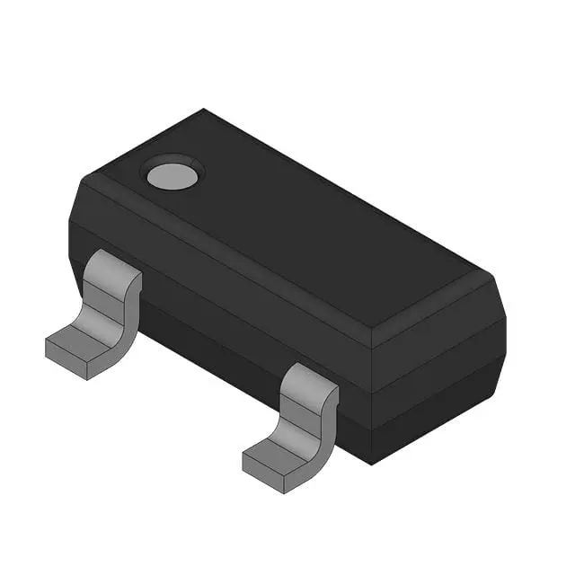
Images are for reference only
MMBFJ309LT1G
RF MOSFET N-CH JFET SOT23-3
- Manufacturer
- Mfr. Part #MMBFJ309LT1G
- Package SOT23-3
- Datasheet
- In Stock6058
100% Original & New
24 Hours ready to ship
365 Days Warranty
RFQ & Get more Discounts
Specifications
| Package | Tape & Reel (TR),Cut Tape (CT),Bulk |
| ProductStatus | Active |
| TransistorType | N-Channel JFET |
| CurrentRating(Amps) | 30mA |
| Voltage-Rated | 25 V |
| Package/Case | TO-236-3, SC-59, SOT-23-3 |
Overview
Description
Key specifications typically include a maximum drain-source voltage (V_DS) of around 30V and a continuous drain current (I_D) rating up to 9A. Its compact package offers ease of integration into circuit designs, and it usually comes in a TO-220 or similar surface-mount configuration.
The MMBFJ309LT1G is often utilized in applications like DC-DC converters, motor drivers, and signal switching, where reliable performance and thermal efficiency are critical. Always refer to the manufacturer's datasheet for detailed electrical characteristics and thermal management guidelines to ensure optimal usage in your specific application.
Features
1. Low Noise: Designed to provide low noise performance, making it suitable for RF and audio applications.
2. High Input Impedance: Offers high input impedance, which minimizes loading on the previous stage, ideal for buffering.
3. Low Gate-Source Cutoff Voltage: Typically has a gate-source cutoff voltage (Vgs) of around -1V, allowing for effective switching.
4. Small Package: Available in a surface-mount SOT-23 package, suitable for high-density applications.
5. Wide Frequency Response: Capable of handling a wide range of frequencies, making it versatile for various circuit designs.
6. Operating Temperature Range: Supports a broad operating temperature range, allowing for use in different environments.
Overall, the MMBFJ309LT1G is well-suited for applications such as amplifiers, switches, and signal processing circuits.
Package
Pinout
1. Gate (G): This is the control terminal of the JFET, used to modulate the current flowing between the drain and source.
2. Source (S): This terminal is where the current enters the JFET from the channel.
3. Drain (D): This terminal is where the current exits the JFET, allowing it to control and amplify signals.
The MMBFJ309LT1G is designed for low-frequency applications and is commonly used in RF amplifiers, switch circuits, and analog signal processing. Its compact package and low noise characteristics make it suitable for various electronic applications.
Manufacturer
Application
Equivalent
Shipping
Shipping MethodsWe
offer global shipping services through DHL, FedEx, TNT, UPS, or any other forwarder of your choice.
Shipping Fee Reference (DHL/FedEx):
DHL: Shipping cost ranges from $25-$45 (0.5kg), with an estimated delivery time of 2-5 business days.
FedEx: Shipping cost ranges from $25-$40 (0.5kg), with an estimated delivery time of 3-7 business days.
UPS: Shipping cost ranges from $25-$45 (0.5kg), with an estimated delivery time of 3-7 business days.
TNT: Shipping cost ranges from $25-$65 (0.5kg), with an estimated delivery time of 3-7 business days.
EMS: Shipping cost ranges from $30-$50 (0.5kg), with an estimated delivery time of 7-15 business days.
Registered Air Mail: Shipping cost is $2-$4 (0.1kg), with an estimated delivery time of 5-20 business days.
Payments
Payment Methods
The Payment term is 100% Prepaid.
Currently, we only accept the below payment methods:
1. PayPal
2. Credit/ Debit Card
3. Wire Transfer
Similar
-
![MX25L3233FM1I-08Q]() MX25L3233FM1I-08Q
MX25L3233FM1I-08Q
Macronix
-
![MX66U1G45GXDI00]() MX66U1G45GXDI00
MX66U1G45GXDI00
Macronix
-
![MX25V4035FZUI]() MX25V4035FZUI
MX25V4035FZUI
Macronix
-
![MX25R3235FZNIL0]() MX25R3235FZNIL0
MX25R3235FZNIL0
Macronix
-
![MX25R6435FBDIL0]() MX25R6435FBDIL0
MX25R6435FBDIL0
Macronix
-
![MX25L25673GMI-08G]() MX25L25673GMI-08G
MX25L25673GMI-08G
Macronix
-
![MX25L25673GMI-10G]() MX25L25673GMI-10G
MX25L25673GMI-10G
Macronix
-
![MX25L12835FZ2I-10G]() MX25L12835FZ2I-10..
MX25L12835FZ2I-10..
Macronix
-
![MX29F040CTI-70G]() MX29F040CTI-70G
MX29F040CTI-70G
Macronix
-
![MX30LF4G18AC-TI]() MX30LF4G18AC-TI
MX30LF4G18AC-TI
Macronix
-
![MX25L1006EMI-10G]() MX25L1006EMI-10G
MX25L1006EMI-10G
Macronix
-
![MX25L4006EM2I-12G]() MX25L4006EM2I-12G
MX25L4006EM2I-12G
Macronix






