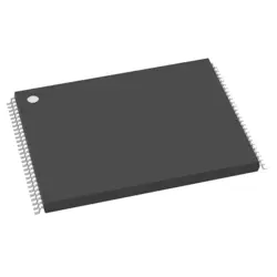
Images are for reference only
MT48LC16M16A2BG-75:D
IC DRAM 256MBIT PAR 54VFBGA
- Manufacturer
- Mfr. Part #MT48LC16M16A2BG-75:D
- Package
- Datasheet MT48LC16M16A2BG-75:D DataSheet
- In Stock3645
100% Original & New
24 Hours ready to ship
365 Days Warranty
RFQ & Get more Discounts
Specifications
| Part Status | Obsolete |
| Base Product Number | MT48LC16M16A2 |
| DigiKey Programmable | Not Verified |
| Memory Type | Volatile |
| Memory Format | DRAM |
| Technology | SDRAM |
| Memory Size | 256Mbit |
| Memory Organization | 16M x 16 |
| Memory Interface | Parallel |
| Clock Frequency | 133 MHz |
| Write Cycle Time - Word, Page | 15ns |
| Voltage - Supply | 3V ~ 3.6V |
| Operating Temperature | 0°C ~ 70°C (TA) |
| Mounting Type | Surface Mount |
| Package | 54-VFBGA |
| Supplier Device Package | 54-VFBGA (8x14) |
| Packaging | Tray |
| Access Time | 5.4 ns |
Overview
Description
This SDRAM operates with a 3.3V power supply and utilizes a synchronous interface, meaning that its operations are synchronized with a clock signal, allowing for precise control over timing and workflows. The device is suitable for use in a wide range of applications, including computing, networking, and consumer electronics, where reliable and fast data access is crucial.
The BG-75:D package indicates a specific form factor and pin configuration for mounting on circuit boards. It includes features like auto precharge, self-refresh, and burst read/write capabilities, enhancing its efficiency and functionality in various use environments.
Features
Package
Pinout
The key functions of the pins include:
- Data Pins (DQ0-DQ15): 16 data input/output pins.
- Address Pins (A0-A12): Address inputs for row and column addresses. Multiplexed to select a location within the DRAM.
- Bank Address Pins (BA0, BA1): Used to select one of the 4 internal banks.
- Control Pins:
- CAS# (Column Address Strobe), RAS# (Row Address Strobe), WE# (Write Enable): Control commands for operation.
- CS# (Chip Select): Activates or deactivates the chip.
- CKE (Clock Enable): Controls the clock signal and power-down modes.
- Clock Pin (CLK): Synchronizes data input and output.
- DQM Pins (DQM0-DQM1): Mask operations for byte control during reads and writes.
- Power Supply Pins (VDD, VSS): Provide power and ground connections.
This configuration allows the SDRAM to perform high-speed, efficient memory operations in a wide range of applications.
Manufacturer
Application
Equivalent
Shipping
Shipping MethodsWe
offer global shipping services through DHL, FedEx, TNT, UPS, or any other forwarder of your choice.
Shipping Fee Reference (DHL/FedEx):
DHL: Shipping cost ranges from $25-$45 (0.5kg), with an estimated delivery time of 2-5 business days.
FedEx: Shipping cost ranges from $25-$40 (0.5kg), with an estimated delivery time of 3-7 business days.
UPS: Shipping cost ranges from $25-$45 (0.5kg), with an estimated delivery time of 3-7 business days.
TNT: Shipping cost ranges from $25-$65 (0.5kg), with an estimated delivery time of 3-7 business days.
EMS: Shipping cost ranges from $30-$50 (0.5kg), with an estimated delivery time of 7-15 business days.
Registered Air Mail: Shipping cost is $2-$4 (0.1kg), with an estimated delivery time of 5-20 business days.
Payments
Payment Methods
The Payment term is 100% Prepaid.
Currently, we only accept the below payment methods:
1. PayPal
2. Credit/ Debit Card
3. Wire Transfer
Similar
-
![MX25L3233FZBI-08Q]() MX25L3233FZBI-08Q
Macronix
-
![MX25L3233FM1I-08Q]() MX25L3233FM1I-08Q
Macronix
-
![MX25V1635FZNI]() MX25V1635FZNI
Macronix
-
![MX29F400CBTI-70G]() MX29F400CBTI-70G
Macronix
-
![MX25V2033FM1I]() MX25V2033FM1I
Macronix
-
![MX30LF2G28AD-TI]() MX30LF2G28AD-TI
Macronix
-
![MX25L25673GMI-08G]() MX25L25673GMI-08G
Macronix
-
![MX25L25673GMI-10G]() MX25L25673GMI-10G
Macronix
-
![MX25L6433FM2I-08G]() MX25L6433FM2I-08G
Macronix
-
![MX29LV160DTTI-70G]() MX29LV160DTTI-70G
Macronix
-
![MX25L25645GXDI-08G]() MX25L25645GXDI-08..
Macronix
-
![MX29LV640ETTI-70G]() MX29LV640ETTI-70G
Macronix