
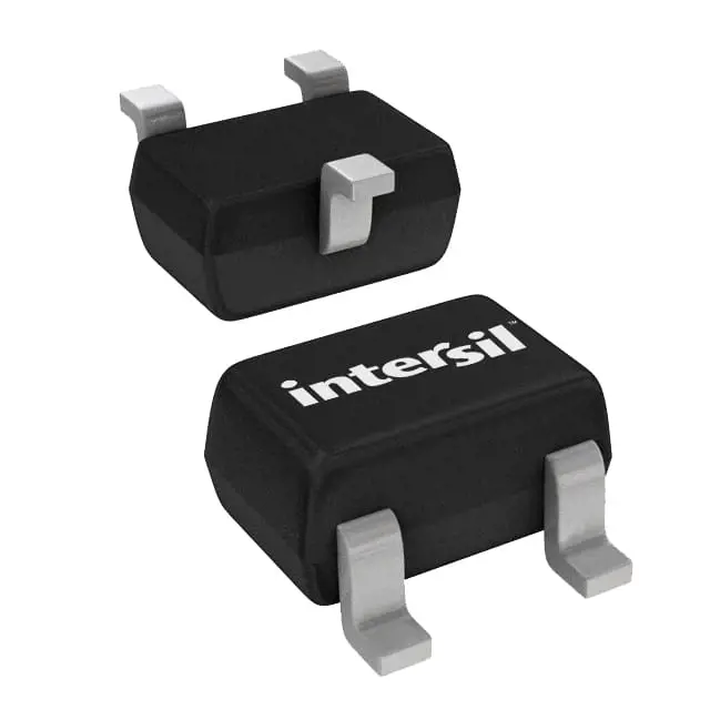
Images are for reference only
MUN5211T1G
TRANS PREBIAS NPN 50V SC70-3
- Manufacturer
- Mfr. Part #MUN5211T1G
- Package SC-70-3
- Datasheet
- In Stock3390
100% Original & New
24 Hours ready to ship
365 Days Warranty
RFQ & Get more Discounts
Specifications
| Package | Tape & Reel (TR),Cut Tape (CT),Bulk |
| ProductStatus | Active |
| TransistorType | NPN - Pre-Biased |
| Current-Collector(Ic)(Max) | 100 mA |
| Voltage-CollectorEmitterBreakdown(Max) | 50 V |
| Resistor-Base(R1) | 10 kOhms |
| Resistor-EmitterBase(R2) | 10 kOhms |
| DCCurrentGain(hFE)(Min)@IcVce | 35 @ 5mA, 10V |
| VceSaturation(Max)@IbIc | 250mV @ 300µA, 10mA |
| Current-CollectorCutoff(Max) | 500nA |
| Power-Max | 202 mW |
| MountingType | Surface Mount |
| Package/Case | SC-70, SOT-323 |
Overview
Description
Features
1. High Integration: Combines multiple functionalities into a single chip, reducing board space and complexity.
2. Low Power Consumption: Optimized for energy efficiency, making it suitable for battery-operated devices.
3. Wide Frequency Range: Supports a broad spectrum of operational frequencies, enhancing versatility in applications.
4. Robust Performance: Delivers reliable performance under varying conditions, ensuring stability and longevity.
5. Advanced Interface Options: Supports multiple communication protocols, facilitating easy integration into existing systems.
6. Temperature Tolerance: Designed to operate effectively across a range of temperatures, suitable for industrial applications.
7. Compact Package Size: Small form factor, allowing integration into space-constrained designs.
Overall, the MUN5211T1G is ideal for applications in wireless communication, IoT devices, and embedded systems, providing a blend of efficiency, performance, and flexibility.
Package
Pinout
1. Gate 1 (G1) - Controls the first N-channel MOSFET.
2. Drain 1 (D1) - The drain terminal for the first MOSFET.
3. Source 1 (S1) - The source terminal for the first MOSFET.
4. Gate 2 (G2) - Controls the second N-channel MOSFET.
5. Drain 2 (D2) - The drain terminal for the second MOSFET.
6. Source 2 (S2) - The source terminal for the second MOSFET.
This device is primarily used for switching applications in power management and signal amplification. Each MOSFET can be independently controlled, making it versatile for various electronic circuit designs.
Manufacturer
Application
Equivalent
Shipping
Shipping MethodsWe
offer global shipping services through DHL, FedEx, TNT, UPS, or any other forwarder of your choice.
Shipping Fee Reference (DHL/FedEx):
DHL: Shipping cost ranges from $25-$45 (0.5kg), with an estimated delivery time of 2-5 business days.
FedEx: Shipping cost ranges from $25-$40 (0.5kg), with an estimated delivery time of 3-7 business days.
UPS: Shipping cost ranges from $25-$45 (0.5kg), with an estimated delivery time of 3-7 business days.
TNT: Shipping cost ranges from $25-$65 (0.5kg), with an estimated delivery time of 3-7 business days.
EMS: Shipping cost ranges from $30-$50 (0.5kg), with an estimated delivery time of 7-15 business days.
Registered Air Mail: Shipping cost is $2-$4 (0.1kg), with an estimated delivery time of 5-20 business days.
Payments
Payment Methods
The Payment term is 100% Prepaid.
Currently, we only accept the below payment methods:
1. PayPal
2. Credit/ Debit Card
3. Wire Transfer
Similar
-
![MX25V1635FZNQ03]() MX25V1635FZNQ03
MX25V1635FZNQ03
Macronix
-
![MX29F400CBTI-70G]() MX29F400CBTI-70G
MX29F400CBTI-70G
Macronix
-
![MX25V4035FZUI]() MX25V4035FZUI
MX25V4035FZUI
Macronix
-
![MX25V2033FM1I]() MX25V2033FM1I
MX25V2033FM1I
Macronix
-
![MX25R3235FZNIL0]() MX25R3235FZNIL0
MX25R3235FZNIL0
Macronix
-
![MX25V16066M2I02]() MX25V16066M2I02
MX25V16066M2I02
Macronix
-
![MX25L8035EM2I-10G]() MX25L8035EM2I-10G
MX25L8035EM2I-10G
Macronix
-
![MX25R6435FBDIL0]() MX25R6435FBDIL0
MX25R6435FBDIL0
Macronix
-
![MX25L25673GMI-08G]() MX25L25673GMI-08G
MX25L25673GMI-08G
Macronix
-
![MX29GL512FHXFI-11G]() MX29GL512FHXFI-11..
MX29GL512FHXFI-11..
Macronix
-
![MX25U25643GZNI00]() MX25U25643GZNI00
MX25U25643GZNI00
Macronix
-
![MX25L2006EM1I-12G]() MX25L2006EM1I-12G
MX25L2006EM1I-12G
Macronix







