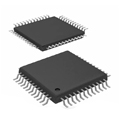

Images are for reference only
NCE4080K
- Manufacturer
- Mfr. Part #NCE4080K
- Package
- Datasheet
- In Stock5911
100% Original & New
24 Hours ready to ship
365 Days Warranty
RFQ & Get more Discounts
Specifications
| Manufacturer | Wuxi NCE Power Semiconductor |
| Package | TO-252-2(DPAK) |
| Operating Temperature | -55℃~+175℃ |
| RDS(on) | 7mΩ@10V,20A |
| Drain to Source Voltage | 40V |
| Pd - Power Dissipation | 80W |
| Current - Continuous Drain(Id) | 80A |
| Reverse Transfer Capacitance (Crss@Vds) | 500pF@20V |
| Input Capacitance(Ciss@Vds) | 5nF@20V |
| Gate Threshold Voltage (Vgs(th)@Id) | 2.5V |
| Gate Charge(Qg) | 61nC |
| Number | 1 N-channel |
Overview
Description
Key topics may include signal processing, microcontroller programming, and the integration of sensors and actuators in electronic projects. Hands-on laboratory work is often a significant component, allowing students to apply theoretical knowledge to real-world scenarios.
Overall, NCE4080K aims to equip students with the necessary skills to design, analyze, and implement complex electronic systems, preparing them for careers in electronics, automation, and related fields.
Features
1. Voltage Rating: Typically supports up to 80V, making it suitable for high-voltage applications.
2. On-Resistance (Rds(on)): Low on-resistance minimizes conduction losses, enhancing efficiency.
3. Current Rating: Capable of handling high continuous current, ideal for demanding applications.
4. Fast Switching: Optimized for rapid switching speeds, reducing transition losses in high-frequency operations.
5. Thermal Performance: Designed with good thermal characteristics, capable of dissipation under high load conditions.
6. Package Options: Available in various packages to accommodate different circuit designs and thermal management needs.
7. Applications: Commonly used in DC-DC converters, motor drives, and power supply circuits.
These features make the NCE4080K a reliable choice for engineers seeking efficient and robust MOSFET solutions.
Package
Pinout
### Pin Count and Functions:
1. Pin 1 (Offset Null): Adjusts the output offset voltage.
2. Pin 2 (Inverting Input A): Input for the first operational amplifier (A).
3. Pin 3 (Non-Inverting Input A): Input for the first operational amplifier (A).
4. Pin 4 (Output A): Output for the first operational amplifier (A).
5. Pin 5 (Ground): Connects to the ground of the circuit.
6. Pin 6 (Output B): Output for the second operational amplifier (B).
7. Pin 7 (Non-Inverting Input B): Input for the second operational amplifier (B).
8. Pin 8 (Inverting Input B): Input for the second operational amplifier (B).
This configuration allows for a variety of applications in signal amplification and conditioning.
Manufacturer
Application
Equivalent
Shipping
Shipping MethodsWe
offer global shipping services through DHL, FedEx, TNT, UPS, or any other forwarder of your choice.
Shipping Fee Reference (DHL/FedEx):
DHL: Shipping cost ranges from $25-$45 (0.5kg), with an estimated delivery time of 2-5 business days.
FedEx: Shipping cost ranges from $25-$40 (0.5kg), with an estimated delivery time of 3-7 business days.
UPS: Shipping cost ranges from $25-$45 (0.5kg), with an estimated delivery time of 3-7 business days.
TNT: Shipping cost ranges from $25-$65 (0.5kg), with an estimated delivery time of 3-7 business days.
EMS: Shipping cost ranges from $30-$50 (0.5kg), with an estimated delivery time of 7-15 business days.
Registered Air Mail: Shipping cost is $2-$4 (0.1kg), with an estimated delivery time of 5-20 business days.
Payments
Payment Methods
The Payment term is 100% Prepaid.
Currently, we only accept the below payment methods:
1. PayPal
2. Credit/ Debit Card
3. Wire Transfer
Similar
-
![MX25L3233FM1I-08Q]() MX25L3233FM1I-08Q
Macronix
-
![MX29F400CBTI-70G]() MX29F400CBTI-70G
Macronix
-
![MX25V2033FM1I]() MX25V2033FM1I
Macronix
-
![MX25V16066M2I02]() MX25V16066M2I02
Macronix
-
![MX30LF2G28AD-TI]() MX30LF2G28AD-TI
Macronix
-
![MX25L25673GMI-10G]() MX25L25673GMI-10G
Macronix
-
![MX25U25643GZNI00]() MX25U25643GZNI00
Macronix
-
![MX25L2006EM1I-12G]() MX25L2006EM1I-12G
Macronix
-
![MX25V1635FM2I]() MX25V1635FM2I
Macronix
-
![MX25L6433FM2I-08G]() MX25L6433FM2I-08G
Macronix
-
![MX25U6435FM2I-10G]() MX25U6435FM2I-10G
Macronix
-
![MX25L12833FM2I-10G]() MX25L12833FM2I-10..
Macronix