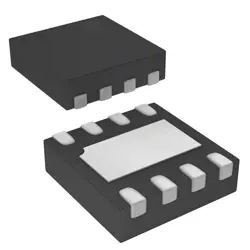
Images are for reference only
NSI8121N0
- Manufacturer
- Mfr. Part #NSI8121N0
- Package
- Datasheet NSI8121N0 DataSheet
- In Stock5545
100% Original & New
24 Hours ready to ship
365 Days Warranty
RFQ & Get more Discounts
Specifications
| Manufacturer | NOVOSENSE |
| Package | SOIC-8 |
| Data Rate(Max) | 150Mbps |
| Default Output | Low Level |
| Isolation Voltage(Vrms) | 3750 |
| CMTI(kV/us) | 150kV/us |
| Number of Forward Channels | 1 |
| Number of Reverse Channels | 1 |
| Operating Temperature | -40℃~+125℃ |
Overview
Description
The device typically operates at a voltage rating of 100V and a continuous drain current that supports robust performance in demanding environments. Key specifications often include a low threshold voltage and a fast recovery time, which help reduce power losses during operation.
Due to its compact package, NSI8121N0 is well-suited for applications that require space-efficient components without compromising on power handling. Its reliability and effectiveness in thermal dissipation further enhance its appeal in high-density circuit designs.
Overall, the NSI8121N0 is a versatile MOSFET choice for engineers looking to improve power efficiency and performance in their electronic designs.
Features
1. Voltage Rating: Offers a maximum drain-source voltage (VDS) of 120V.
2. Current Rating: Supports continuous drain current (ID) of up to 30A, suitable for high-current applications.
3. RDS(on): Low on-resistance (typically 0.12 ohms), which reduces power loss and improves efficiency.
4. Gate Threshold Voltage: Low gate threshold voltage (VGS(th)) around 2-4V, allowing for efficient drive with lower gate voltages.
5. Package Type: Typically available in TO-220 or similar packages for effective thermal dissipation.
6. Switching Speed: Fast switching capabilities, making it suitable for high-frequency applications.
7. Thermal Resistance: Good thermal performance, allowing for higher power dissipation.
These features make the NSI8121N0 ideal for use in switching power supplies, motor drivers, and other power electronic applications.
Package
Pinout
The key functions of its pins are as follows:
1. VIN: Input voltage supply.
2. GND: Ground reference.
3. SW: Switch node connection to the inductor.
4. VOUT: Output voltage connection.
5. COMP: Compensation network connection for stability.
6. FB: Feedback pin to regulate output voltage.
7. EN: Enable pin to turn the device on/off.
8. SS: Soft-start pin to control the ramp-up time of the output voltage.
This IC is used in applications such as battery-powered devices, portable electronics, and other low-voltage power supply needs.
Manufacturer
Application
Equivalent
Shipping
Shipping MethodsWe
offer global shipping services through DHL, FedEx, TNT, UPS, or any other forwarder of your choice.
Shipping Fee Reference (DHL/FedEx):
DHL: Shipping cost ranges from $25-$45 (0.5kg), with an estimated delivery time of 2-5 business days.
FedEx: Shipping cost ranges from $25-$40 (0.5kg), with an estimated delivery time of 3-7 business days.
UPS: Shipping cost ranges from $25-$45 (0.5kg), with an estimated delivery time of 3-7 business days.
TNT: Shipping cost ranges from $25-$65 (0.5kg), with an estimated delivery time of 3-7 business days.
EMS: Shipping cost ranges from $30-$50 (0.5kg), with an estimated delivery time of 7-15 business days.
Registered Air Mail: Shipping cost is $2-$4 (0.1kg), with an estimated delivery time of 5-20 business days.
Payments
Payment Methods
The Payment term is 100% Prepaid.
Currently, we only accept the below payment methods:
1. PayPal
2. Credit/ Debit Card
3. Wire Transfer
Similar
-
![MX25L3233FM1I-08Q]() MX25L3233FM1I-08Q
MX25L3233FM1I-08Q
Macronix
-
![MX25V1635FZNI]() MX25V1635FZNI
MX25V1635FZNI
Macronix
-
![MX29F400CBTI-70G]() MX29F400CBTI-70G
MX29F400CBTI-70G
Macronix
-
![MX25V5126FM1I]() MX25V5126FM1I
MX25V5126FM1I
Macronix
-
![MX25V4035FZUI]() MX25V4035FZUI
MX25V4035FZUI
Macronix
-
![MX25L8035EM2I-10G]() MX25L8035EM2I-10G
MX25L8035EM2I-10G
Macronix
-
![MX25L25673GMI-08G]() MX25L25673GMI-08G
MX25L25673GMI-08G
Macronix
-
![MX25L25673GMI-10G]() MX25L25673GMI-10G
MX25L25673GMI-10G
Macronix
-
![MX25R1635FZUIH0]() MX25R1635FZUIH0
MX25R1635FZUIH0
Macronix
-
![MX25U3232FZBI02]() MX25U3232FZBI02
MX25U3232FZBI02
Macronix
-
![MX25U6435FM2I-10G]() MX25U6435FM2I-10G
MX25U6435FM2I-10G
Macronix
-
![MX25L12835FZ2I-10G]() MX25L12835FZ2I-10..
MX25L12835FZ2I-10..
Macronix