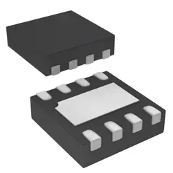
Images are for reference only
NT5CC64M16GP-DII
1Gbit 1.35V 800MHz DDR3L SDRAM VFBGA-96 Memory (ICs) RoHS
- Manufacturer
- Mfr. Part #NT5CC64M16GP-DII
- Package
- Datasheet NT5CC64M16GP-DII DataSheet
- In Stock6341
100% Original & New
24 Hours ready to ship
365 Days Warranty
RFQ & Get more Discounts
Specifications
| Packaging | VFBGA-96 |
| Clock Frequency | 800MHz |
| Memory Format | DDR3L SDRAM |
| Memory Size | 1Gbit |
| Operating temperature | -40℃~+95℃ |
| Voltage - Supply | 1.35V |
Overview
Description
The device employs a 4-bit prefetch architecture, which enhances its data transfer efficiency. It features various operational modes, including burst lengths of 4 and 8, and supports various power-saving modes to improve energy efficiency during operation. The NT5CC64M16GP-DII is commonly used in PCs, laptops, and other devices requiring reliable and fast memory performance. Its design adheres to JEDEC standards, ensuring compatibility with a wide range of motherboards and systems.
Features
1. Type: DDR3 SDRAM (Double Data Rate Type 3 Synchronous Dynamic Random Access Memory).
2. Density: 1GB (Gigabyte) capacity, composed of 64M x 16 bits configuration.
3. Speed: Operates at a data rate of 1066 MT/s (Million Transfers per second).
4. Voltage: Typically operates at 1.5V, enhancing energy efficiency.
5. Package: Available in a standard FBGA (Fine-pitch Ball Grid Array) package, facilitating compact design.
6. Applications: Suitable for a range of applications including laptops, desktops, and embedded systems.
7. Operating Temperature: Designed for industrial-grade reliability, often with a wide temperature range.
This module is ideal for enhancing memory performance in various computing environments while ensuring stability and efficiency.
Package
Pinout
The key functions of the pins include:
- Address Pins (A0-A11): These pins are used to select memory addresses.
- Data Pins (DQ0-DQ15): These are bi-directional data pins for data input/output.
- Control Pins: These include Chip Select (CS), Write Enable (WE), Read Enable (OE), and Clock (CLK), which manage memory operations.
- Power and Ground Pins: VDD and VSS pins provide the necessary power supply and ground connections.
This DRAM is commonly used in various applications, including consumer electronics and computing devices, due to its efficient performance and compatibility with standard memory protocols.
Manufacturer
Application
Equivalent
Shipping
Shipping MethodsWe
offer global shipping services through DHL, FedEx, TNT, UPS, or any other forwarder of your choice.
Shipping Fee Reference (DHL/FedEx):
DHL: Shipping cost ranges from $25-$45 (0.5kg), with an estimated delivery time of 2-5 business days.
FedEx: Shipping cost ranges from $25-$40 (0.5kg), with an estimated delivery time of 3-7 business days.
UPS: Shipping cost ranges from $25-$45 (0.5kg), with an estimated delivery time of 3-7 business days.
TNT: Shipping cost ranges from $25-$65 (0.5kg), with an estimated delivery time of 3-7 business days.
EMS: Shipping cost ranges from $30-$50 (0.5kg), with an estimated delivery time of 7-15 business days.
Registered Air Mail: Shipping cost is $2-$4 (0.1kg), with an estimated delivery time of 5-20 business days.
Payments
Payment Methods
The Payment term is 100% Prepaid.
Currently, we only accept the below payment methods:
1. PayPal
2. Credit/ Debit Card
3. Wire Transfer
Similar
-
![MX25L3233FM1I-08Q]() MX25L3233FM1I-08Q
MX25L3233FM1I-08Q
Macronix
-
![MX25V16066M1I02]() MX25V16066M1I02
MX25V16066M1I02
Macronix
-
![MX25V16066M2I02]() MX25V16066M2I02
MX25V16066M2I02
Macronix
-
![MX25R6435FBDIL0]() MX25R6435FBDIL0
MX25R6435FBDIL0
Macronix
-
![MX25U51279GXDR00]() MX25U51279GXDR00
MX25U51279GXDR00
Macronix
-
![MX25R1635FZUIH0]() MX25R1635FZUIH0
MX25R1635FZUIH0
Macronix
-
![MX25V1635FM2I]() MX25V1635FM2I
MX25V1635FM2I
Macronix
-
![MX25U3232FZBI02]() MX25U3232FZBI02
MX25U3232FZBI02
Macronix
-
![MX25L12833FZ2I-10G]() MX25L12833FZ2I-10..
MX25L12833FZ2I-10..
Macronix
-
![MX25L12833FZNI-10G]() MX25L12833FZNI-10..
MX25L12833FZNI-10..
Macronix
-
![MX25L12835FZ2I-10G]() MX25L12835FZ2I-10..
MX25L12835FZ2I-10..
Macronix
-
![MX30LF4G18AC-TI]() MX30LF4G18AC-TI
MX30LF4G18AC-TI
Macronix