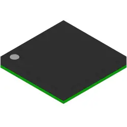
Images are for reference only
PC28F00BP30EFA
NOR Flash PARALLEL NOR MLC 128MX16 TBGA DDP
- Manufacturer
- Mfr. Part #PC28F00BP30EFA
- Package
- Datasheet
- In Stock16046
100% Original & New
24 Hours ready to ship
365 Days Warranty
RFQ & Get more Discounts
Specifications
| Packaging | Tray |
| Standard Pack Qty | 1800 |
Overview
Description
Key features include a voltage range of 2.7V to 3.6V, a typical access time of 70 ns, and support for multiple programming modes, including byte-alterable and sector erase. It supports a variety of interface protocols, making it compatible with various microprocessors.
The chip is designed for high endurance and reliability, capable of withstanding numerous write-erase cycles, making it ideal for applications where data retention and longevity are critical. Its compact form factor allows for integration into space-constrained designs. Overall, the PC28F00BP30EFA is a versatile memory solution for various applications, including automotive, industrial, and telecommunications.
Features
1. Density: 512Mb capacity suitable for various embedded applications.
2. Architecture: Organization in 8 bits x 8 bits or 16 bits x 16 bits, allowing flexible interfacing.
3. Access Speed: Supports fast read access times, promoting efficient data retrieval.
4. Programming: Features sector-based programming, enabling selective data modification.
5. Endurance: Typically offers high endurance with up to 100,000 program/erase cycles per sector.
6. Data Retention: Guaranteed data retention of up to 20 years.
7. Interface: Commonly supports standard parallel interfaces for easy integration.
8. Temperature Range: Designed to operate over a wide temperature range, making it suitable for various environments.
These features make the PC28F00BP30EFA ideal for applications in consumer electronics, automotive, and industrial sectors where reliability and performance are crucial.
Package
Pinout
The pin count is 32, and the functions of the pins are as follows:
1. Address Inputs (A0-A18): 19 pins for addressing memory locations.
2. Data Inputs/Outputs (D0-D7): 8 pins for data transfer.
3. Chip Enable (CE): Activates the chip for operation.
4. Output Enable (OE): Allows data output to be enabled.
5. Write Enable (WE): Controls writing operations.
6. Byte/Word (B/W): Selects byte or word mode.
7. Reset (RESET): Resets the device.
8. Vcc: Power supply input.
9. GND: Ground connection.
This device is typically used in applications requiring non-volatile memory for firmware or data storage.
Manufacturer
Application
Equivalent
Shipping
Shipping MethodsWe
offer global shipping services through DHL, FedEx, TNT, UPS, or any other forwarder of your choice.
Shipping Fee Reference (DHL/FedEx):
DHL: Shipping cost ranges from $25-$45 (0.5kg), with an estimated delivery time of 2-5 business days.
FedEx: Shipping cost ranges from $25-$40 (0.5kg), with an estimated delivery time of 3-7 business days.
UPS: Shipping cost ranges from $25-$45 (0.5kg), with an estimated delivery time of 3-7 business days.
TNT: Shipping cost ranges from $25-$65 (0.5kg), with an estimated delivery time of 3-7 business days.
EMS: Shipping cost ranges from $30-$50 (0.5kg), with an estimated delivery time of 7-15 business days.
Registered Air Mail: Shipping cost is $2-$4 (0.1kg), with an estimated delivery time of 5-20 business days.
Payments
Payment Methods
The Payment term is 100% Prepaid.
Currently, we only accept the below payment methods:
1. PayPal
2. Credit/ Debit Card
3. Wire Transfer
Similar
-
![MX25R8035FM1IL0]() MX25R8035FM1IL0
Macronix
-
![MX25V1635FZNI]() MX25V1635FZNI
Macronix
-
![MX25V16066M1I02]() MX25V16066M1I02
Macronix
-
![MX25V16066M2I02]() MX25V16066M2I02
Macronix
-
![MX25L25673GMI-08G]() MX25L25673GMI-08G
Macronix
-
![MX25L25673GMI-10G]() MX25L25673GMI-10G
Macronix
-
![MX29GL512FHXFI-11G]() MX29GL512FHXFI-11..
Macronix
-
![MX25U51279GXDR00]() MX25U51279GXDR00
Macronix
-
![MX25R1635FZUIH0]() MX25R1635FZUIH0
Macronix
-
![MX25L12833FZNI-10G]() MX25L12833FZNI-10..
Macronix
-
![MX25U25645GXDI00]() MX25U25645GXDI00
Macronix
-
![MX29F040CTI-70G]() MX29F040CTI-70G
Macronix