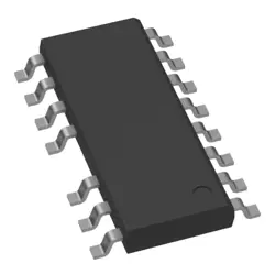
Images are for reference only
SN65LVDS31PW
IC DRIVER 4/0 16TSSOP
- Manufacturer
- Mfr. Part #SN65LVDS31PW
- Package TSSOP (PW)-16
- Datasheet
- In Stock2327
100% Original & New
24 Hours ready to ship
365 Days Warranty
RFQ & Get more Discounts
Specifications
| Package | Tube |
| Series | 65LVDS |
| ProductStatus | Active |
| Type | Driver |
| Protocol | LVDS |
| NumberofDrivers/Receivers | 4/0 |
| DataRate | 400Mbps |
| Voltage-Supply | 3V ~ 3.6V |
| OperatingTemperature | -40°C ~ 85°C |
| MountingType | Surface Mount |
| Package/Case | 16-TSSOP (0.173, 4.40mm Width) |
Overview
Description
Key attributes include a wide common-mode voltage range and low power consumption, which make it ideal for various industrial and consumer applications, such as telecommunications, data communication, and video transmission. The SN65LVDS31PW also includes built-in fail-safe mechanisms that ensure reliable operation under fault conditions. Its small package size and compatibility with standard LVDS signaling make it a popular choice for designers looking to implement high-speed data links in their systems.
Features
1. Data Rate: Supports data rates up to 400 Mbps.
2. Input Voltage Range: Operates over a wide input voltage range for robust performance.
3. Low Power Consumption: Features a low supply current, making it energy-efficient.
4. Single Supply Operation: Requires a single 3.3V power supply.
5. High Noise Immunity: Offers excellent common-mode noise rejection and is suitable for noisy environments.
6. Differential Inputs: Utilizes differential signaling to minimize electromagnetic interference.
7. Wide Temperature Range: Designed to operate in harsh environments, with a temperature range from -40°C to 85°C.
8. Output Compatibility: Compatible with LVTTL output levels, allowing easy interfacing with digital devices.
These features make the SN65LVDS31PW ideal for applications in telecommunications, data acquisition systems, and high-speed serial communications.
Package
Pinout
1. Differential Output Pins (OUT+ and OUT-): These are used for transmitting LVDS signals.
2. Single-Ended Input Pins (IN+ and IN-): These accept the differential input signals.
3. Supply Voltage (Vcc): This pin is for connecting to the power supply.
4. Ground (GND): This pin is used for the ground reference.
5. Enable Pin (EN): This pin allows for enabling or disabling the driver.
6. Common Mode Voltage (VCM): This pin is used to set the common mode voltage.
7. Thermal Pad: Provides heat dissipation.
The SN65LVDS31PW is designed for high-speed data transmission, making it suitable for applications like video and high-speed communications, while minimizing signal degradation and power consumption.
Manufacturer
Application
Equivalent
Shipping
Shipping MethodsWe
offer global shipping services through DHL, FedEx, TNT, UPS, or any other forwarder of your choice.
Shipping Fee Reference (DHL/FedEx):
DHL: Shipping cost ranges from $25-$45 (0.5kg), with an estimated delivery time of 2-5 business days.
FedEx: Shipping cost ranges from $25-$40 (0.5kg), with an estimated delivery time of 3-7 business days.
UPS: Shipping cost ranges from $25-$45 (0.5kg), with an estimated delivery time of 3-7 business days.
TNT: Shipping cost ranges from $25-$65 (0.5kg), with an estimated delivery time of 3-7 business days.
EMS: Shipping cost ranges from $30-$50 (0.5kg), with an estimated delivery time of 7-15 business days.
Registered Air Mail: Shipping cost is $2-$4 (0.1kg), with an estimated delivery time of 5-20 business days.
Payments
Payment Methods
The Payment term is 100% Prepaid.
Currently, we only accept the below payment methods:
1. PayPal
2. Credit/ Debit Card
3. Wire Transfer
Similar
-
![MX25R8035FM1IL0]() MX25R8035FM1IL0
MX25R8035FM1IL0
Macronix
-
![MX25V5126FM1I]() MX25V5126FM1I
MX25V5126FM1I
Macronix
-
![MX25R3235FZNIL0]() MX25R3235FZNIL0
MX25R3235FZNIL0
Macronix
-
![MX29GL512FHXFI-11G]() MX29GL512FHXFI-11..
MX29GL512FHXFI-11..
Macronix
-
![MX25U51279GXDR00]() MX25U51279GXDR00
MX25U51279GXDR00
Macronix
-
![MX25L2006EM1I-12G]() MX25L2006EM1I-12G
MX25L2006EM1I-12G
Macronix
-
![MX25L12833FZNI-10G]() MX25L12833FZNI-10..
MX25L12833FZNI-10..
Macronix
-
![MX29F040CTI-70G]() MX29F040CTI-70G
MX29F040CTI-70G
Macronix
-
![MX25L25735FMI-10G]() MX25L25735FMI-10G
MX25L25735FMI-10G
Macronix
-
![MX30LF4G18AC-TI]() MX30LF4G18AC-TI
MX30LF4G18AC-TI
Macronix
-
![MX25L1006EMI-10G]() MX25L1006EMI-10G
MX25L1006EMI-10G
Macronix
-
![MX66U1G45GMI00]() MX66U1G45GMI00
MX66U1G45GMI00
Macronix